#photonics
Engineers Develop Flexible and Stretchable Photonic Devices
Engineers at MIT have developed a new material that can be repeatedly stretched and flexed without losing its optical properties.
Researchers at MIT and several other institutions have developed a method for making photonic devices — similar to electronic devices but based on light rather than electricity — that can bend and stretch without damage. The devices could find uses in cables to connect computing devices, or in diagnostic and monitoring systems that could be attached to the skin or implanted in the body, flexing easily with the natural tissue.
The findings, which involve the use of a specialized kind of glass called chalcogenide, are described in two papers by MIT Associate Professor Juejun Hu and more than a dozen others at MIT, the University of Central Florida, and universities in China and France. The paper is slated for publication soon in Light: Science and Applications.
Hu, who is the Merton C. Flemings Associate Professor of Materials Science and Engineering, says that many people are interested in the possibility of optical technologies that can stretch and bend, especially for applications such as skin-mounted monitoring devices that could directly sense optical signals. Such devices might, for example, simultaneously detect heart rate, blood oxygen levels, and even blood pressure.
Post link
First integrated laser on lithium niobate chip
For all the recent advances in integrated lithium niobate photonic circuits—from frequency combs to frequency converters and modulators—one big component has remained frustratingly difficult to integrate: lasers.
Long haul telecommunication networks, data center optical interconnects, and microwave photonic systems all rely on lasers to generate an optical carrier used in data transmission. In most cases, lasers are stand-alone devices, external to the modulators, making the whole system more expensive and less stable and scalable.
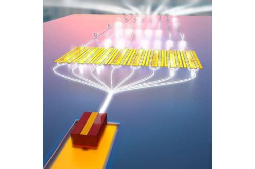
Now, researchers from the Harvard John A. Paulson School of Engineering and Applied Sciences (SEAS) in collaboration with industry partners at Freedom Photonics and HyperLight Corporation, have developed the first fully integrated high-power laser on a lithium niobate chip, paving the way for high-powered telecommunication systems, fully integrated spectrometers, optical remote sensing, and efficient frequency conversion for quantum networks, among other applications.
Post link
Telecommunications light amplifier could strengthen integrity of transmitted data
Imagine a dim light which is insufficiently bright enough to illuminate a room. An amplifier for such a light would increase the brightness by increasing the number of photons emitted. Photonics researchers have created such a high gain optical amplifier that is compact enough to be placed on a chip. The developed amplifier, when used within an optical interconnect such as a transceiver or fiber optic network, would help to efficiently increase the power of the transmitted light before it is completely depleted through optical losses.
Besides having the potential to replace bulky, expensive amplifiers used today for the study of attosecond science and ultrafast optical information processing, the newly developed nanoscale-amplifier also provides a critical element to the optical interconnects toolkit, potentially providing regenerative amplification in short to long range interconnects. This work was a collaborative effort between researchers at the Singapore University of Technology and Design (SUTD), A*STAR Data Storage Institute and the Massachusetts Institute of Technology. Details appeared in Nature Communications on January 4th 2017.
Post link
Lighting the way for new materials
What happens when gold and silver just don’t cut it anymore? You turn to metallic alloys, which are what Army researchers are using to develop new designer materials with a broad range of capabilities for our Soldiers.
This is exactly what scientists Dr. David Baker and Dr. Joshua McClure from the U.S. Army Research Laboratory are doing to lighten the load and enhance the power of Soldier devices used on the battlefield.
Their research, conducted in collaboration with Prof. Marina Leite and Dr. Chen Gong at the University of Maryland and Prof. Alexandre Rocha at the Universidade Estadual Paulista in Brazil, was recently featured on the cover of the Sept. 4 issue of Advanced Optical Materials.
The research paper, “Band Structure Engineering by Alloying for Photonics,” focuses on control of the optical and plasmonic properties of gold and silver alloys by changing alloy chemical composition.
Post link
Artificial material protects light states on smallest length scales
Light not only plays a key role as an information carrier for optical computer chips, particularly for the next generation of quantum computers. Its lossless guidance around sharp corners on tiny chips and the precise control of its interaction with other light are the focus of research worldwide. Scientists at Paderborn University have now demonstrated the spatial confinement of a light wave to a point smaller than the wavelength in a topological photonic crystal. These are artificial electromagnetic materials that facilitate robust manipulation of light. The state is protected by special properties and is important for quantum chips, for example. The findings have now been published in Science Advances.
Topological crystals function on the basis of specific structures, the properties of which remain largely unaffected by disturbances and deviations. While in normal photonic crystals the effects needed for light manipulation are fragile and can be affected by defects in the material structure, for example, in topological photonic crystals, the conditions are protected from this. The topological structures allow properties such as unidirectional light propagation and increased robustness for guiding photons, features that are crucial for future light-based technologies.
Post link
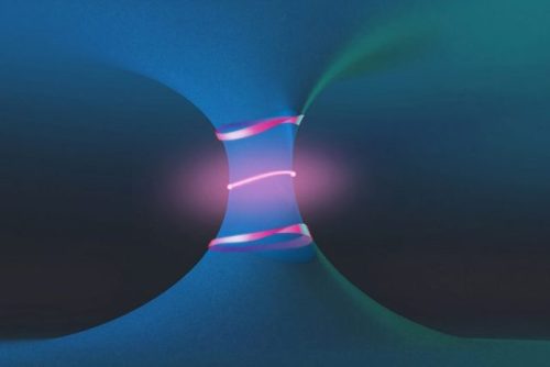
This Slinky lookalike ‘hyperlens’ helps us see tiny objects
It looks like a Slinky suspended in motion.
Yet this photonics advancement – called a metamaterial hyperlens – doesn’t climb down stairs.
Instead, it improves our ability to see tiny objects.
Described in a research paper published today by the journal Nature Communications, the hyperlens may someday help detect some of the most lethal forms of cancer.
It could also lead to advancements in nanoelectronic manufacturing and boost scientists’ ability to examine single molecules – a development with implications in physics, chemistry, biology and other fields.
“There is a great need in health care, nanotechnology and other areas to improve our ability to see tiny objects that elude even the most powerful optical systems. The hyperlens we are developing is, potentially, a giant step toward solving this problem,” says Natalia Litchinitser, PhD, professor of electrical engineering at the University at Buffalo and the paper’s lead author.
Post link
Integrated metasurface converts colors of light over broadband inside a waveguide
One of the biggest challenges in developing integrated photonic circuits—which use light rather than electrons to transport information—is to control the momentum of light. Colors of light travel at different speeds through a material but in order for light to be converted between colors, it needs to have the same momentum or phase.
Many devices have been designed to momentum-match or phase-match light at various points throughout an integrated circuit but what if the phase-matching process could be circumvented all together in certain cases?
Researchers at the Harvard John A. Paulson School of Engineering and Applied Sciences, together with collaborators from the Fu Foundation School of Engineering and Applied Science at Columbia University, have developed a system to convert one wavelength of light into another without the need to phase match.
The research was published in Nature Communications.
“For any wavelength conversion process to be efficient, it has to be carefully designed to phase match, and it only works at a single wavelength,” said Marko Loncar, the Tiantsai Lin Professor of Electrical Engineering at SEAS and senior author of the paper. “The devices shown in this work, in contrast, do not need to satisfy the phase-matching requirement, and can convert light in a broad colorrange.”
Post link
Scientists Observe New Exotic Phenomena in Photonic Crystals
Topological effects, such as those found in crystals whose surfaces conduct electricity while their bulk does not, have been an exciting topic of physics research in recent years and were the subject of the 2016 Nobel Prize in physics. Now, a team of researchers at MIT and elsewhere has found novel topological phenomena in a different class of systems — open systems, where energy or material can enter or be emitted, as opposed to closed systems with no such exchange with the outside.
This could open up some new realms of basic physics research, the team says, and might ultimately lead to new kinds of lasers and other technologies.
The results are being reported this week in the journal Science, in a paper by recent MIT graduate Hengyun “Harry” Zhou, MIT visiting scholar Chao Peng (a professor at Peking University), MIT graduate student Yoseob Yoon, recent MIT graduates Bo Zhen and Chia Wei Hsu, MIT Professor Marin Soljačić, the Francis Wright Davis Professor of Physics John Joannopoulos, the Haslam and Dewey Professor of Chemistry Keith Nelson, and the Lawrence C. and Sarah W. Biedenharn Career Development Assistant Professor Liang Fu.
Post link
Invisibility cloak with photonic crystals
Metamaterials made from metal elements initially proposed for constructing invisibility cloaks, did not solve some important cloaking problems.
There are three challenges remaining. The first is controlling anisotropy – the variable behavior of propagating waves in different directions of the cloak medium. It’s also important to make sure that the cloak materials can operate at microwave and optical wave frequencies. Finally, researchers have to decrease losses that restrict the size of hidden objects.
Elena Semouchkina, an associate professor of electrical and computer engineering, and her graduate students have developed several novel approaches to making invisibility cloaks more practical. Their latest work, published in a special issue of Journal of Optics on transformation optics, looks at a promising new way to manipulate electromagnetic waves to make objects appear invisible. The team developed an approach using photonic crystals.
Post link
Ultrafast optical-magnetic memory device
Magnetic random-access memory (MRAM) technology offers substantial potential towards next-generation universal memory architecture. However, state-of-the-art MRAMs are still fundamentally constrained by a sub-nanosecond speed limitation, which has remained a long-lasting scientific challenge in the spintronics R&D. In this double doctorate project, Luding Wang experimentally demonstrated a fully-functional picosecond opto-MRAM building block device, by integrating ultrafast photonics with spintronics.
MRAM development bottlenecks
Have you ever experienced an unexpected shutdown of your computer, losing documents in the process that you have spent hours working on? Magnetic random-access memory (MRAM) technology focuses on manipulating electron spin to deal with such a technical glitch. Inside MRAM bits, data are written by switching the direction nanomagnets. Thus, MRAM allows data to be saved in an enduring manner when the power is off, computers to boot faster, and the devices consume less power.
Post link


