#spintronics
Magnetic surprise revealed in ‘magic-angle’ graphene
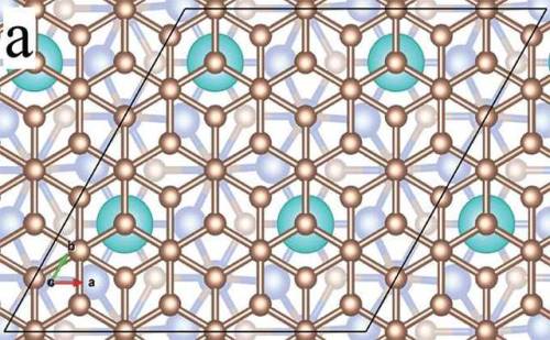
When two sheets of the carbon nanomaterial graphene are stacked together at a particular angle with respect to each other, it gives rise to some fascinating physics. For instance, when this so-called “magic-angle graphene” is cooled to near absolute zero, it suddenly becomes a superconductor, meaning it conducts electricity with zero resistance.
Now, a research team from Brown University has found a surprising new phenomenon that can arise in magic-angle graphene. In research published in the journal Science, the team showed that by inducing a phenomenon known as spin-orbit coupling, magic-angle graphene becomes a powerful ferromagnet.
“Magnetism and superconductivity are usually at opposite ends of the spectrum in condensed matter physics, and it’s rare for them to appear in the same material platform,” said Jia Li, an assistant professor of physics at Brown and senior author of the research. “Yet we’ve shown that we can create magnetism in a system that originally hosts superconductivity. This gives us a new way to study the interplay between superconductivity and magnetism, and provides exciting new possibilities for quantum science research.”
Post link
Scientists move graphene closer to transistor applications
Scientists at the U.S. Department of Energy’s Ames Laboratory were able to successfully manipulate the electronic structure of graphene, which may enable the fabrication of graphene transistors— faster and more reliable than existing silicon-based transistors.
The researchers were able to theoretically calculate the mechanism by which graphene’s electronic band structure could be modified with metal atoms. The work will guide experimentally the use of the effect in layers of graphene with rare-earth metal ions “sandwiched” (or intercalated) between graphene and its silicon carbide substrate. Because the metal atoms are magnetic the additions can also modify the use of graphene for spintronics.
“We are discovering new and more useful versions of graphene,” said Ames Laboratory senior scientist Michael C. Tringides. “We found that the placement of the rare earth metals below graphene, and precisely where they are located, in the layers between graphene and its substrate, is critical to manipulating the bands and tune the band gap.”
Post link
Researchers observe electrons zipping around in crystals
The end of the silicon age has begun. As computer chips approach the physical limits of miniaturization and power-hungry processors drive up energy costs, scientists are looking to a new crop of exotic materials that could foster a new generation of computing devices that promise to push performance to new heights while skimping on energy consumption.
Unlike current silicon-based electronics, which shed most of the energy they consume as waste heat, the future is all about low-power computing. Known as spintronics, this technology relies on a quantum physical property of electrons – up or down spin – to process and store information, rather than moving them around with electricity as conventional computing does.
On the quest to making spintronic devices a reality, scientists at the University of Arizona are studying an exotic crop of materials known as transition metal dichalcogenides, or TMDs. TMDs have exciting properties lending themselves to new ways of processing and storing information and could provide the basis of future transistors and photovoltaics – and potentially even offer an avenue toward quantum computing.
For example, current silicon-based solar cells convert realistically only about 25 percent of sunlight into electricity, so efficiency is an issue, says Calley Eads, a fifth-year doctoral student in the UA’s Department of Chemistry and Biochemistry who studies some of the properties of these new materials. “There could be a huge improvement there to harvest energy, and these materials could potentially do this,” she says.
Post link
By encoding information in photons via their spin, “photonic” computers could be orders of magnitude faster and efficient than their current-day counterparts. Likewise, encoding information in the spin of electrons, rather than just their quantity, could make “spintronic” computers with similar a…
Diamonds show promise for spintronic devices
New experiments demonstrate the potential for diamond as a material for spintronics
Conventional electronics rely on controlling electric charge. Recently, researchers have been exploring the potential for a new technology, called spintronics, that relies on detecting and controlling a particle’s spin. This technology could lead to new types of more efficient and powerful devices.
In a paper published in Applied Physics Letters, from AIP Publishing, researchers measured how strongly a charge carrier’s spin interacts with a magnetic field in diamond. This crucial property shows diamond as a promising material for spintronic devices.
Diamond is attractive because it would be easier to process and fabricate into spintronic devices than typical semiconductor materials, said Golrokh Akhgar, a physicist at La Trobe University in Australia. Conventional quantum devices are based on multiple thin layers of semiconductors, which require an elaborate fabrication process in an ultrahigh vacuum.
“Diamond is normally an extremely good insulator,” Akhgar said. But, when exposed to hydrogen plasma, the diamond incorporates hydrogen atoms into its surface. When a hydrogenated diamond is introduced to moist air, it becomes electrically conductive because a thin layer of water forms on its surface, pulling electrons from the diamond. The missing electrons at the diamond surface behave like positively charged particles, called holes, making the surface conductive.
Post link
Magnetism under the magnifying glass
Being able to determine magnetic properties of materials with sub-nanometer precision would greatly simplify development of magnetic nano-structures for future spintronic devices. In an article published in Nature Communications Uppsala physicists make a big step towards this goal – they propose and demonstrate a new measurement method capable to detect magnetism from areas as small as 0.5 nm2.
Due to the ever-growing demand for more powerful electronic devices the next generation spintronic components must have functional units that are only a few nanometers large. It is easier to build a new spintronic device, if we can see it in a sufficient detail. This becomes more and more tricky with the rapid advance of nano-technologies, especially when we need not only an overall picture “how the thing looks,” but also know its physical properties at nano-scale. One of instruments capable of such detailed look is a transmission electron microscope.
Electron microscope is a unique experimental tool offering to scientists and engineers a wealth of information about all kinds of materials. Differently from optical microscopes, it uses electrons to study the materials, and thanks to that it achieves an enormous magnification. For example, in crystals one can even observe individual columns of atoms. Electron microscopes routinely provide information about structure, composition and chemistry of materials. Recently researchers found ways to use electron microscopes also for measuring magnetic properties. There, however, atomic resolution has not been reached so far.
Post link
Ultrafast optical-magnetic memory device
Magnetic random-access memory (MRAM) technology offers substantial potential towards next-generation universal memory architecture. However, state-of-the-art MRAMs are still fundamentally constrained by a sub-nanosecond speed limitation, which has remained a long-lasting scientific challenge in the spintronics R&D. In this double doctorate project, Luding Wang experimentally demonstrated a fully-functional picosecond opto-MRAM building block device, by integrating ultrafast photonics with spintronics.
MRAM development bottlenecks
Have you ever experienced an unexpected shutdown of your computer, losing documents in the process that you have spent hours working on? Magnetic random-access memory (MRAM) technology focuses on manipulating electron spin to deal with such a technical glitch. Inside MRAM bits, data are written by switching the direction nanomagnets. Thus, MRAM allows data to be saved in an enduring manner when the power is off, computers to boot faster, and the devices consume less power.
Post link


