#nanostructures
Better, bolder printing with silicon nanostructures
From textbooks to artwork to newspapers, printed items are a part of our everyday life. But the ink used in today’s printers are limited in colors and resolution. Now in a new study in ACS’ journal Nano Letters, scientists have found a way to expand the printable color spectrum with a novel nanostructure system.
The current color range for computers and printers is based on the sRGB (standard Red Green Blue) color space, which was developed in 1996 by Microsoft and Hewlett-Packard. But the hues in the sRGB system only encompass a subset of colors that the human eye can see. Researchers have been trying to develop a better system to surpass sRGB that would broaden the printable color spectrum while maintaining high resolution.
For example, they have used metallic nanostructures for color printing, but this has resulted in either high-resolution images with less-rich colors, or images with vivid colors but lower resolution. Also, the use of metals like silver and gold would likely be too expensive for wide adoption. So researchers have turned to silicon because it has unique properties that might be optimal for expanding computer and printing colors at a lower price. But so far, silicon color systems have shown poor color saturation and range. So Joel Yang and colleagues wanted to design a novel silicon nanostructure that could potentially overcome these limitations and compete with the sRGB system.
Post link
Silicon Anode Nanostructure Generates New Potential for Lithium-Ion Batteries
Scientists reveal a new nanostructure that could revolutionize technology in batteries and beyond.
- New research has identified a nanostructure that improves the anode in lithium-ion batteries
- Instead of using graphite for the anode, the researchers turned to silicon: a material that stores more charge but is susceptible to fracturing
- The team made the silicon anode by depositing silicon atoms on top of metallic nanoparticles
- The resulting nanostructure formed arches, increasing the strength and structural integrity of the anode
- Electrochemical tests showed the lithium-ion batteries with the improved silicon anodes had a higher charge capacity and longer lifespan
New research conducted by the Okinawa Institute of Science and Technology Graduate University (OIST) has identified a specific building block that improves the anode in lithium-ion batteries. The unique properties of the structure, which was built using nanoparticle technology, are revealed and explained today (February 5, 2021) in Communications Materials.
Post link
How a tetrahedral substance can be more symmetrical than a spherical atom: A new type of symmetry
Scientists at Tokyo Institute of Technology have theoretically demonstrated that special tetrahedron nanostructures composed of certain metals have a higher degree of symmetry than the geometrical symmetry of spherical atoms. Nanomaterials with unique and unprecedented electrical and magnetic properties arising from this symmetry will be developed and used for next-generation electronic devices.
[…]
Studying symmetry, one of the most fundamental concepts in physics and chemistry, can facilitate a deeper understanding of the laws shaping our universe.
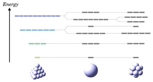
Atoms naturally have the highest degree of geometrical symmetry, corresponding to the spherical symmetry. An interesting property often arising from symmetry is a high degree of degeneracy–a characteristic of quantum energy levels wherein a given energy level can correspond simultaneously to two or more different states in a quantum system. Degeneracy gives rise to properties including high conductivity and magnetism, which could be exploited to create novel electronic materials. Unfortunately, given the limitations of geometrical symmetry, no substance is known to have a higher degree of degeneracy than spherical atoms (Fig. 1). But what if substances could have a different type of symmetry leading to a higher degree of degeneracy? How could such a symmetry be explained?
Post link
Laser additive manufacturing of Si/ZrO2 tunable crystalline phase 3D nanostructures
A new publication from Opto-Electronic Advances reviews laser additive manufacturing of Si/ZrO2 tunable crystalline phase 3D nanostructures.
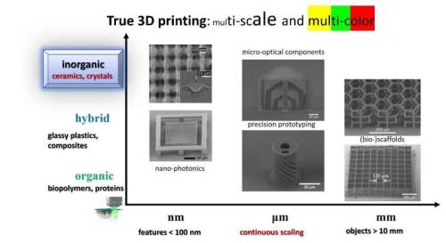
A route for laser nano-printing of 3D crystalline structures was developed employing ultrafast laser lithography, used as additive manufacturing tool for producing true 3D nanostructures, and combined with high temperature thermal post-treatment, converting the printed material into fully inorganic substance.
The inter-disciplinary experimental work revealed the potential of tuning the resulting ceramic structure into distinct crystalline phases, such as cristobalite, SiO2, ZrSiO4, m-ZrO2, t-ZrO2. The proposed approach achieved below 60 nm for individual feature dimensions without any beam shaping or complex exposure techniques, thus making it reproducible with other established standard or custom-made laser direct writing setups. The principle is compatible with commercially available platforms (for instance: Nanoscribe, MultiPhoton Optics, Femtika, Workshop of Photonics, UpNano, MicroLight, and others). Figure 1 graphically summarizes the approach, involved procedure steps, and resulting outcome.
Post link
Tripling the efficiency of solar-based hydrogen fuel generation with metallic nanostructures that slow down light
Hydrogen gas, an important synthetic feedstock, is poised to play a key role in renewable energy technology; however, its credentials are undermined because most is currently sourced from fossil fuels, such as natural gas. A KAUST team has now found a more sustainable route to hydrogen fuel production using chaotic, light-trapping materials that mimic natural photosynthetic water splitting.
The complex enzymes inside plants are impractical to manufacture, so researchers have developed photocatalysts that employ high-energy, hot electrons to cleave water molecules into hydrogen and oxygen gas. Recently, nanostructured metals that convert solar electrons into intense, wave-like plasmon resonances have attracted interest for hydrogen production. The high-speed metal plasmons help transfer carriers to catalytic sites before they relax and reduce catalytic efficiency.
Getting metal nanoparticles to respond to the entire broadband spectrum of visible light is challenging. “Plasmonic systems have specific geometries that trap light only at characteristic frequencies,” explains Andrea Fratalocchi, who led the research. “Some approaches try to combine multiple nanostructures to soak up more colors, but these absorptions take place at different spatial locations so the sun’s energy is not harvested very efficiently.”
Post link
Integrated metasurface converts colors of light over broadband inside a waveguide
One of the biggest challenges in developing integrated photonic circuits—which use light rather than electrons to transport information—is to control the momentum of light. Colors of light travel at different speeds through a material but in order for light to be converted between colors, it needs to have the same momentum or phase.
Many devices have been designed to momentum-match or phase-match light at various points throughout an integrated circuit but what if the phase-matching process could be circumvented all together in certain cases?
Researchers at the Harvard John A. Paulson School of Engineering and Applied Sciences, together with collaborators from the Fu Foundation School of Engineering and Applied Science at Columbia University, have developed a system to convert one wavelength of light into another without the need to phase match.
The research was published in Nature Communications.
“For any wavelength conversion process to be efficient, it has to be carefully designed to phase match, and it only works at a single wavelength,” said Marko Loncar, the Tiantsai Lin Professor of Electrical Engineering at SEAS and senior author of the paper. “The devices shown in this work, in contrast, do not need to satisfy the phase-matching requirement, and can convert light in a broad colorrange.”
Post link
Precisely tailoring the dynamics of upconversion luminescence
A team of researchers led by Professors Hong Zhang (photonic nanochemistry) and Evert Jan Meijer (computational chemistry) of the University of Amsterdam’s Van ’t Hoff Institute for Molecular Sciences has significantly improved the fundamental understanding of photon upconversion in nanoparticles. Through the collaborative approach of advanced spectroscopy and theoretical modelling they were able to establish that the migration of excitation energy greatly affects the upconversion dynamics. In a recent publication in Angewandte Chemie the researchers describe how ‘dopant ions spatially separated’ (DISS) nanostructures can be used for tailoring the upconversion dynamics.
Upconversion is a process in which one photon is emitted upon absorption of several photons of lower energy. It thus 'jacks’ the light from lower to higher frequencies. Typically upconversion materials are doped with lanthanide ions. These are able to shift the near infrared (NIR) light of an economic continuous wave milliwatt laser towards higher, visible frequencies and even into the ultraviolet (UV) spectral region. Potential applications in super resolution spectroscopy, high density data storage, anti-counterfeiting and biological imaging and photo-induced therapy.
Upconversion luminescence dynamics has long been believed to be determined solely by the emitting ions and their interactions with neighbouring sensitizing ions. The current research shows that this does not hold for nanostructures. Zhang, Meijer and co-workers demonstrate that in nanocrystals the luminescence time behaviour is seriously affected by the migration process of the excitation energy.
Post link
Silk Fibers May Represent Natural Metamaterials, Capable of light Confinement
New research has demonstrated how the nano-architecture of a silkworm’s fiber causes “Anderson localization of light,” a discovery that could lead to various innovations and a better understanding of light transport and heat transfer.
The discovery also could help create synthetic materials and structures that realize the phenomenon, named after Nobel laureate Philip Anderson, whose theory describes how electrons can be brought to a complete halt in materials due to their “scattering and defects.” The new findings relate not to electrons, but to light transport.
Researchers demonstrated how the nano-architecture of the silk fibers is capable of light “confinement,” a trait that could provide a range of technological applications including innovations that harness light for new types of medical therapies and biosensing. This light-confinement effect in biological and natural tissue, which was unexpected, is made possible by the Anderson localization of light, said Young Kim, an associate professor in Purdue University’s Weldon School of Biomedical Engineering.
The new findings suggest silk fibers may represent “natural metamaterials” and “natural metastructures,” Kim said.
Post link
New research opening for atomically thin metal nanostructures
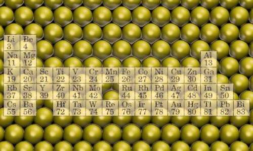
Researchers at the Nanoscience Center at the University of Jyväskylä, Finland, have made a new opening in nanomaterial research. Opening’s essence resides in the exclusive use of metallic elements in flat, atomically thin nanostructures.
The best known flat nanomaterial is graphene. Graphene is stable because the non-metallic element carbon prefers covalent, directional bonds that effectively cause structural planarity. Metallic bonds are less directional, whereby metals often coalesce into compact clusters. However, recent experiments suggest that, by using pores in other nanostructures, even metals can be stabilized into atomically thin planes.
Inspired by these experimental indications, researchers at the Nanoscience Center, University of Jyväskylä, used computer simulations to predict systematically the properties of atomically thin structures made exclusively from metallic elements.
“We made a new opening in material research, which was basic research, but highly rewarding as such,” says postdoctoral researcher Janne Nevalaita. “One could say that we hit on an untouched estate, bulldozed it and created a foundation. Now others can build solid scientific structures based on that foundation,” he continues.
Post link
Hybrid nanomaterials bristle with potential
By combining multiple nanomaterials into a single structure, scientists can create hybrid materials that incorporate the best properties of each component and outperform any single substance. A controlled method for making triple-layered hollow nanostructures has now been developed at KAUST. The hybrid structures consist of a conductive organic core sandwiched between layers of electrocatalytically active metals: their potential uses range from better battery electrodes to renewable fuel production.
Although several methods exist to create two-layer materials, making three-layered structures has proven much more difficult, says Peng Wang from the Water Desalination and Reuse Center who co-led the current research with Professor Yu Han, member of the Advanced Membranes and Porous Materials Center at KAUST. The researchers developed a new, dual-template approach, explains Sifei Zhuo, a postdoctoral member of Wang’s team.
The researchers grew their hybrid nanomaterial directly on carbon paper—a mat of electrically conductive carbon fibers. They first produced a bristling forest of nickel cobalt hydroxyl carbonate (NiCoHC) nanowires onto the surface of each carbon fiber (image 1). Each tiny inorganic bristle was coated with an organic layer called hydrogen substituted graphdiyne (HsGDY) (image 2).
Post link
New screen coating makes reading in sunlight a lot easier—the secret? Moth eyes
Screens on even the newest phones and tablets can be hard to read outside in bright sunlight. Inspired by the nanostructures found on moth eyes, researchers have developed a new antireflection film that could keep people from having to run to the shade to look at their mobile devices.
The antireflection film exhibits a surface reflection of just .23 percent, much lower than the iPhone’s surface reflection of 4.4 percent, for example. Reflection is the major reason it’s difficult to read a phone screen in bright sunlight, as the strong light reflecting off the screen’s surface washes out the display.
Researchers led by Shin-Tson Wu of the College of Optics and Photonics, University of Central Florida (CREOL), report on their new antireflection coating in Optica, The Optical Society’s journal for high impact research.
“Using our flexible anti-reflection film on smartphones and tablets will make the screen bright and sharp, even when viewed outside,” said Wu. “In addition to exhibiting low reflection, our nature-inspired film is also scratch resistant and self-cleaning, which would protect touch screens from dust and fingerprints.”
Post link
Aluminum “Octopods” – Shape Matters for Light-Activated Nanocatalysts
Study: Pointed tips on aluminum ‘octopods’ increase catalytic reactivity.
Points matter when designing nanoparticles that drive important chemical reactions using the power of light.
Researchers at Rice University’s Laboratory for Nanophotonics (LANP) have long known that a nanoparticle’s shape affects how it interacts with light, and their latest study shows how shape affects a particle’s ability to use light to catalyze important chemical reactions.
In a comparative study, LANP graduate students Lin Yuan and Minhan Lou and their colleagues studied aluminum nanoparticles with identical optical properties but different shapes. The most rounded had 14 sides and 24 blunt points. Another was cube-shaped, with six sides and eight 90-degree corners. The third, which the team dubbed “octopod,” also had six sides, but each of its eight corners ended in a pointed tip.
Post link


