Nanotechnology is the area of science and innovation concerned with material of less than 100 nanometers. Specifically, it involves the control and manipulation of individual atoms and molecules. On this day in 1979, IBM created the smallest electronic circuit elements ever reported. The nano devices had a thickness of only 100 by 200 atomic diameters – that’s smaller than the fibers of a human nerve. This breakthrough was one of the first steps in the still-ongoing development of nanotechnology. Today, IBM scientists continue to explore and improve the design of semiconductors and computer chips, making them smaller, smarter and more energy efficient. It’s another way IBM is investing in practical technology development for the future.
Heated magnetic nanoparticles may be the future of eradicating cancer cells without harming healthy tissue, according to research from the University of Buffalo, USA. The nanoparticles strike tumours with significant heat under a low magnetic field.
Hao Zeng, Professor of Physics at Buffalo, said, ‘The main accomplishment of our work is the greatly enhanced heating performance of nanoparticles under low-field conditions suitable for clinical applications. The best heating power we obtained is close to the theoretical limit, greatly surpassing some of the best performing particles that other research teams have produced.’
Targeting technologies would first direct nanoparticles to tumours within the patient’s body. Exposure to an alternating magnetic field would prompt the particles’ magnetic orientation to flip back and forth hundreds of thousands of times a second, causing them to warm up as they absorb energy from the electromagnetic field and convert it to thermal energy.
Two particles have been tested – manganese-cobalt-ferrite and zinc ferrite. While the manganese particle reached maximum heating power under high magnetic fields, the biocompatible zinc ferrite was efficieny under an ultra-low field.
While this form of treatment, known as magnetic nanoparticle hyperthermia, is not new, the Buffalo-designed particles are able to generate heat several times faster than the current standard.
Harvesting solar fuels through a bacterium’s unusual appetite for gold
A bacterium named Moorella thermoacetica won’t work for free. But UC Berkeley researchers have figured out it has an appetite for gold. And in exchange for this special treat, the bacterium has revealed a more efficient path to producing solar fuels through artificial photosynthesis.
M. thermoacetica first made its debut as the first non-photosensitive bacterium to carry out artificial photosynthesis in a study led by Peidong Yang, a professor in UC Berkeley’s College of Chemistry. By attaching light-absorbing nanoparticles made of cadmium sulfide (CdS) to the bacterial membrane exterior, the researchers turned M. thermoacetica into a tiny photosynthesis machine, converting sunlight and carbon dioxide into useful chemicals.
Now Yang and his team of researchers have found a better way to entice this CO2-hungry bacterium into being even more productive. By placing light-absorbing gold nanoclusters inside the bacterium, they have created a biohybrid system that produces a higher yield of chemical products than previously demonstrated. The research, funded by the National Institutes of Health, was published on Oct. 1 in Nature Nanotechnology.
A team of researchers have demonstrated the viability of the direct piezoelectric effect in a thin film Bismuth Ferrite Material for the first time. The work, published in Nanoscale entitles “Direct and Converse Piezoelectric Responses at the Nanoscale from Epitaxial BiFeO3 Thin Films Grown by Polymer Assisted Deposition” which has gained the cover letter of such journal.
[…]
In this particular research, the BFO was scanned in a novel methodology named “Direct Piezoelectric Force Microscopy” DPFM, a new AFM mode invented in 2017
(https://www.nature.com/articles/s41467-017-01361-2 ). The material in this mode is stressed by the AFM tip with nanometric size. The tip applies a force in the range of hundreds of microNewton and measures the generated charge that is created by the material. For the case of BFO material, the piezoelectric characteristics were collected when the tip crosses antiparallel domain configurations, see the following video for a 3D representation of the tip crossing such configuration: https://youtu.be/ir3W2Vk8hCs
Rice University nanoscientists have demonstrated a new catalyst that can convert ammonia into hydrogen fuel at ambient pressure using only light energy, mainly due to a plasmonic effect that makes the catalyst more efficient.
[…]
A study from Rice’s Laboratory for Nanophotonics (LANP) in this week’s issue of Science describes the new catalytic nanoparticles, which are made mostly of copper with trace amounts of ruthenium metal. Tests showed the catalyst benefited from a light-induced electronic process that significantly lowered the “activation barrier,” or minimum energy needed, for the ruthenium to break apart ammonia molecules.
The research comes as governments and industry are investing billions of dollars to develop infrastructure and markets for carbon-free liquid ammonia fuel that will not contribute to greenhouse warming. But the researchers say the plasmonic effect could have implications beyond the “ammonia economy.”
UCLA materials scientists and colleagues have discovered that perovskites, a class of promising materials that could be used for low-cost, high-performance solar cells and LEDs, have a previously unutilized molecular component that can further tune the electronic property of perovskites.
Named after Russian mineralogist Lev Perovski, perovskite materials have a crystal-lattice structure of inorganic molecules like that of ceramics, along with organic molecules that are interlaced throughout. Up to now, these organic molecules appeared to only serve a structural function and could not directly contribute to perovskites’ electronic performance.
Led by UCLA, a new study shows that when the organic molecules are designed properly, they not only can maintain the crystal lattice structure, but also contribute to the materials’ electronic properties. This discovery opens up new possibilities to improve the design of materials that will lead to better solar cells and LEDs. The study detailing the research was recently published in Science.
Our consumer products, such as food, cosmetics, and clothes, might be filled with nanomaterials — unbeknownst to us. The use of nanomaterials remains unregulated and they do not show up in lists of ingredients. This is a cause of concern since nanomaterials can be more dangerous than COVID-19 in the long term if no safety action is taken: they are tricky to measure, they enter our food chain and, most alarmingly, they can penetrate cells and accumulate in our organs.
Nanotechnology is appearing everywhere, to change our daily lives. Thanks to applications of nanotechnology, we can treat many diseases so efficiently that they’ll soon be a thing of the past. We also have materials that are 100 times stronger than steel, batteries that last 10 times longer than before, solar panels that yield twice as much energy than old ones, skincare products that keep us looking young, not to mention self-cleaning cars, windows, and clothes. These used to be the stuff of science fiction and Hollywood movies, but are now the reality we live in.
Nanotechnology has the potential to become the next industrial revolution. The global market for nanomaterials is growing, estimated at 11 million tonnes at a market value of 20 billion euros. The current direct employment in the nanomaterial sector is estimated between 300,000 and 400,000 in Europe alone.
When two sheets of the carbon nanomaterial graphene are stacked together at a particular angle with respect to each other, it gives rise to some fascinating physics. For instance, when this so-called “magic-angle graphene” is cooled to near absolute zero, it suddenly becomes a superconductor, meaning it conducts electricity with zero resistance.
Now, a research team from Brown University has found a surprising new phenomenon that can arise in magic-angle graphene. In research published in the journal Science, the team showed that by inducing a phenomenon known as spin-orbit coupling, magic-angle graphene becomes a powerful ferromagnet.
“Magnetism and superconductivity are usually at opposite ends of the spectrum in condensed matter physics, and it’s rare for them to appear in the same material platform,” said Jia Li, an assistant professor of physics at Brown and senior author of the research. “Yet we’ve shown that we can create magnetism in a system that originally hosts superconductivity. This gives us a new way to study the interplay between superconductivity and magnetism, and provides exciting new possibilities for quantum science research.”
A Quantum Dot (QD) is a nanometer-sized semiconductor nanocrystal that has unique optical properties such as the ability to emit light in the range of optical frequencies depending on its size. QDs have already been applied to practical optoelectronic applications including light-emitting displays, solar cells, photodetectors, and lasers.
In general, QDs have two distinct energy bands in which electrons can exist. They are the so-called “valence band” where electrons are fully occupied and the “conduction band” where electrons are empty, respectively. The gap between these two bands is called the “band gap,” where electrons cannot exist. Upon photoexcitation by light with higher energy than the band gap, electrons within the valence band can be excited and jump into the conduction band. A vacancy formed in the valence band after this process is called a “hole,” which is defined as a carrier having a positive charge.
A hole usually pairs with an electron in the conduction band and forms a quasi-particle called an “exciton” that is bound via Coulomb interaction. After formation, the exciton can recombine spontaneously and emit light with the same energy as the band gap. The most important parameter in this process is the “transition dipole moment,” which is an electric dipole moment associated with the transition between the two states. Typically, the larger this quantity, the greater the recombinationrate.
Microscopic electric fields govern a remarkable variety of phenomena in condensed matter and their ultrafast evolutions drive plasmonics, phononics and highspeed nanoelectronics. Access to high-frequency electric waveforms is of crucial importance to diverse disciplines in nanoscience and technology, yet, microscopic measurements are still severely limited.
In a new paper published in Light: Science & Applications, a team of scientists, led by Prof. Georg Herink from the University of Bayreuth, Germany, and co-workers from the University of Melbourne, Australia, has introduced a new THz microscope for imaging ultrafast electric waveforms encoded in the visible luminescence of nanocrystal probes. Strong electric fields modulate the emission yield of nanocrystals and enable the detection of THz near-field waveforms by microscopy of visible photons in the far-field.
The researchers generated ultrafast electric fields inside gold structures using intense Terahertz pulses. A layer of semiconductor nanocrystals covering the samples is excited by ultrashort visible pulses and shows modulated visible emission depending on the momentary local THz electric field. Fundamentally, this probing of electric fields via luminescence yield is enabled by the quantum-confined Stark effect in quantum dots, generating the contrast mechanism of the scheme termed Quantum-Probe Field Microscopy (QFIM). While scanning the temporal delay between THz excitation and optical pulses, an optical fluorescence microscope captures snapshots of the modulated local emission and generates movies of the local fieldevolution.
While working with helium nanodroplets, scientists at the Department of Ion Physics and Applied Physics led by Fabio Zappa and Paul Scheier have come across a surprising phenomenon: When the ultracold droplets hit a hard surface, they behave like drops of water. Ions with which they were previously doped thus remain protected on impact and are not neutralized.
At the Department of Ion Physics and Applied Physics, Paul Scheier’s research group has been using helium nanodroplets to study ions with methods of mass spectrometry for around 15 years. Using a supersonic nozzle, tiny, superfluid helium nanodroplets can be produced with temperatures of less than one degree Kelvin. They can very effectively be doped with atoms and molecules. In the case of ionized droplets, the particles of interest are attached to the charges, which are then measured in the mass spectrometer. During their experiments, the scientists have now stumbled upon an interesting phenomenon that has fundamentally changed their work. “For us, this was a gamechanger,” says Fabio Zappa from the nano-bio-physics team. “Everything at our lab is now done with this newly discovered method.” The researchers have now published the results of their studies in Physical Review Letters.
From textbooks to artwork to newspapers, printed items are a part of our everyday life. But the ink used in today’s printers are limited in colors and resolution. Now in a new study in ACS’ journal Nano Letters, scientists have found a way to expand the printable color spectrum with a novel nanostructure system.
The current color range for computers and printers is based on the sRGB (standard Red Green Blue) color space, which was developed in 1996 by Microsoft and Hewlett-Packard. But the hues in the sRGB system only encompass a subset of colors that the human eye can see. Researchers have been trying to develop a better system to surpass sRGB that would broaden the printable color spectrum while maintaining high resolution.
For example, they have used metallic nanostructures for color printing, but this has resulted in either high-resolution images with less-rich colors, or images with vivid colors but lower resolution. Also, the use of metals like silver and gold would likely be too expensive for wide adoption. So researchers have turned to silicon because it has unique properties that might be optimal for expanding computer and printing colors at a lower price. But so far, silicon color systems have shown poor color saturation and range. So Joel Yang and colleagues wanted to design a novel silicon nanostructure that could potentially overcome these limitations and compete with the sRGB system.
Researchers at MIT have developed a condensation-based method that could create stable nanoscale emulsions.
The reluctance of oil and water to mix together and stay that way is so well-known that it has become a cliché for describing any two things that do not go together well. Now, a new finding from researchers at MIT might turn that expression on its head, providing a way to get the two substances to mix and remain stable for long periods — no shaking required. The process may find applications in pharmaceuticals, cosmetics, and processed foods, among other areas.
The new process involves cooling a bath of oil containing a small amount of a surfactant (a soap-like substance), and then letting water vapor from the surrounding air condense onto the oil surface. Experiments have shown that this can produce tiny, uniform water droplets on the surface that then sink into the oil, and their size can be controlled by adjusting the proportion of surfactant. The findings, by MIT graduate student Ingrid Guha, former postdoc Sushant Anand, and associate professor Kripa Varanasi, are reported in the journal Nature Communications.
As anyone who has ever used salad dressing knows, no matter how vigorously the mixture gets shaken, the oil and the vinegar (a water-based solution) will separate within minutes. But for many uses, including new drug-delivery systems and food-processing methods, it’s important to be able to get oil in water (or water in oil) to form tiny droplets — only a few hundred nanometers across, too small to see with the naked eye — and to have them stay tiny rather than coalescing into larger droplets and eventually separating from the other liquid.
A new form of 3-D-printed material made by combining commonly-used plastics with carbon nanotubes is tougher and lighter than similar forms of aluminium, scientists say.
The material could lead to the development of safer, lighter and more durable structures for use in the aerospace, automotive, renewables and marine industries.
In a new paper published in the journal Materials & Design, a team led by University of Glasgow engineers describe how they have developed a new plate-lattice cellular metamaterial capable of impressive resistance to impacts.
Metamaterials are a class of artificially-created cellular solids, designed and engineered to manifest properties which do not occur in the natural world.
Scientists reveal a new nanostructure that could revolutionize technology in batteries and beyond.
New research has identified a nanostructure that improves the anode in lithium-ion batteries
Instead of using graphite for the anode, the researchers turned to silicon: a material that stores more charge but is susceptible to fracturing
The team made the silicon anode by depositing silicon atoms on top of metallic nanoparticles
The resulting nanostructure formed arches, increasing the strength and structural integrity of the anode
Electrochemical tests showed the lithium-ion batteries with the improved silicon anodes had a higher charge capacity and longer lifespan
New research conducted by the Okinawa Institute of Science and Technology Graduate University (OIST) has identified a specific building block that improves the anode in lithium-ion batteries. The unique properties of the structure, which was built using nanoparticle technology, are revealed and explained today (February 5, 2021) in Communications Materials.
Current silicon-based computing technology is energy-inefficient. Information and communications technology is projected to use over 20% of global electricity production by 2030. So finding ways to decarbonise technology is an obvious target for energy savings. Professor Paolo Radaelli from Oxford’s Department of Physics, working with Diamond Light Source, the U.K.“s national synchrotron, has been leading research into more efficient alternatives to silicon. His group’s surprising findings are published in Nature in an article titled "Antiferromagnetic half-skyrmions and bimerons at room temperature.” Some of the antiferromagnetic textures they have found could emerge as prime candidates for low-energy antiferromagnetic spintronics at room temperature.
Researchers have been working for a long time on alternative technologies to silicon. Oxides of common metals such as iron and copper are natural targets because they are already a technology staple, present in silicon-based computers, meaning there is a high chance of compatibility between the two technologies. Although oxides are great for storing information, they are not good at moving information around—a necessity for computation. However, one property of oxides that has emerged is that many are magnetic, which means it might be possible to move magnetic bits around, both in oxides and in other magnets, with very little energy required.
Improving the sensitivity of light sensors or the efficiency of solar cells requires fine-tuning of light capturing. KAUST researchers have used complex geometry to develop tiny shell-shaped coverings that can increase the efficiency and speed of photodetectors.
Many optical-cavity designs have been investigated to seek efficiencies of light: either by trapping the electromagnetic wave or by confining light to the active region of the device to increase absorption. Most employ simple micrometer- or nanometer-scale spheres in which the light propagates around in circles on the inside of the surface, known as a whispering gallery mode.
Former KAUST scientist Der-Hsien Lien, now a postdoctoral researcher at the University of California, Berkeley, and his colleagues from China, Australia and the U.S. demonstrate that a more complex geometry comprising convex nanoscale shells improves the performance of photodetectors by increasing the speed at which they operate and enabling them to detect light from all directions.
Surface effects play an important role in the operation of some devices, explains KAUST principal investigator, Jr-Hau He. Nanomaterials offer a way to improve performance because of their high surface-to-volume ratio. “However, although nanomaterials have greater sensitivity in light detection compared to the bulk, the light–matter interactions are weaker because they are thinner,” describes He. “To improve this, we design structures for trapping light.”
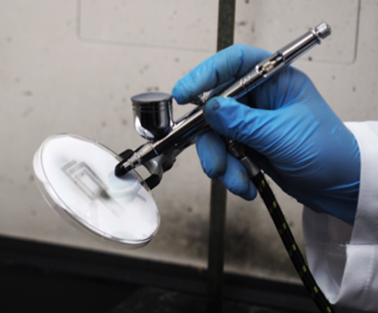
by Yury Gogotsi, Asia Sarycheva, and Babak Anasori
Spraying an antenna onto a flat surface. Drexel University Nanomaterials Lab, CC BY-ND
Hear the word “antenna” and you might think about rabbit ears on the top of an old TV or the wire that picks up radio signals for a car. But an antenna can be much smaller – even invisible. No matter its shape or size, an antenna is crucial for communication, transmitting and receiving radio signals between devices. As portable electronics become increasingly common, antennas must, too.
Wearable monitors, flexible smart clothes, industrial sensors and medical sensors will be much more effective if their antennas are lightweight and flexible – and possibly even transparent. We and our collaborators have developed a type of material that offers many more options for connecting antennas to devices – including spray-painting them on walls or clothes.
Scientists at Tokyo Institute of Technology have theoretically demonstrated that special tetrahedron nanostructures composed of certain metals have a higher degree of symmetry than the geometrical symmetry of spherical atoms. Nanomaterials with unique and unprecedented electrical and magnetic properties arising from this symmetry will be developed and used for next-generation electronic devices.
[…]
Studying symmetry, one of the most fundamental concepts in physics and chemistry, can facilitate a deeper understanding of the laws shaping our universe.
Atoms naturally have the highest degree of geometrical symmetry, corresponding to the spherical symmetry. An interesting property often arising from symmetry is a high degree of degeneracy–a characteristic of quantum energy levels wherein a given energy level can correspond simultaneously to two or more different states in a quantum system. Degeneracy gives rise to properties including high conductivity and magnetism, which could be exploited to create novel electronic materials. Unfortunately, given the limitations of geometrical symmetry, no substance is known to have a higher degree of degeneracy than spherical atoms (Fig. 1). But what if substances could have a different type of symmetry leading to a higher degree of degeneracy? How could such a symmetry be explained?
Printed electronics use standard printing techniques to manufacture electronic devices on different substrates like glass, plastic films, and paper. Interest in this area is growing because of the potential to create cheaper circuits more efficiently than conventional methods. A new study by researchers at Soonchunhyang University in South Korea, published in AIP Advances, provides insights into the processing of copper nanoparticle ink with green laser light.
Kye-Si Kwon and his colleagues previously worked with silver nanoparticle ink, but they turned to copper (derived from copper oxide) as a possible low-cost alternative. Metallic inks composed of nanoparticles hold an advantage over bulk metals because of their lower melting points. Although the melting point of copper is about 1,083 degrees Celsius in bulk, according to Kwon, copper nanoparticles can be brought to their melting point at just 150 to 500 C—through a process called sintering. Then, they can be merged and bound together.
Kwon’s group concentrates on photonic approaches for heating nanoparticles by the absorption of light. “A laser beam can be focused on a very small area, down to the micrometer level,” explained Kwon and doctorate student Md. Khalilur Rahman. Heat from the laser serves two main purposes: converting copper oxide into copper and promoting the conjoining of copper particles through melting.


 is a nanometer-sized")