#crystal growth
Scientists observe nanowires as they grow
X-ray experiments reveal exact details of self-catalyzed growth for the first time
At DESY’s X-ray source PETRA III, scientists have followed the growth of tiny wires of gallium arsenide live. Their observations reveal exact details of the growth process responsible for the evolving shape and crystal structure of the crystalline nanowires. The findings also provide new approaches to tailoring nanowires with desired properties for specific applications. The scientists, headed by Philipp Schroth of the University of Siegen and the Karlsruhe Institute of Technology (KIT), present their findings in the journal Nano Letters. The semiconductor gallium arsenide (GaAs) is widely used, for instance in infrared remote controls, the high-frequency components of mobile phones and for converting electrical signals into light for fibre optical transmission, as well as in solar panels for deployment in spacecraft.
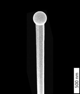
To fabricate the wires, the scientists employed a procedure known as the self-catalysed Vapour-Liquid-Solid (VLS) method, in which tiny droplets of liquid gallium are first deposited on a silicon crystal at a temperature of around 600 degrees Celsius. Beams of gallium atoms and arsenic molecules are then directed at the wafer, where they are adsorpted and dissolve in the gallium droplets. After some time, the crystalline nanowires begin to form below the droplets, whereby the droplets are gradually pushed upwards. In this process, the gallium droplets act as catalysts for the longitudinal growth of the wires. “Although this process is already quite well established, it has not been possible until now to specifically control the crystal structure of the nanowires produced by it. To achieve this, we first need to understand the details of how the wires grow,” emphasises co-author Ludwig Feigl from KIT.
Post link


