#gallium
Search for new semiconductors heats up with gallium oxide
University of Illinois electrical engineers have cleared another hurdle in high-power semiconductor fabrication by adding the field’s hottest material – beta-gallium oxide – to their arsenal. Beta-gallium oxide is readily available and promises to convert power faster and more efficiently than today’s leading semiconductor materials – gallium nitride and silicon, the researchers said.
Their findings are published in the journal ACS Nano.
Flat transistors have become about as small as is physically possible, but researchers addressed this problem by going vertical. With a technique called metal-assisted chemical etching – or MacEtch – U. of I. engineers used a chemical solution to etch semiconductor into 3D fin structures. The fins increase the surface area on a chip, allowing for more transistors or current, and can therefore handle more power while keeping the chip’s footprint the same size.
Developed at the U. of I., the MacEtch method is superior to traditional “dry” etching techniques because it is far less damaging to delicate semiconductor surfaces, such as beta-gallium oxide, researchers said.
“Gallium oxide has a wider energy gap in which electrons can move freely,” said the study’s lead author Xiuling Li, a professor of electrical and computer engineering. “This energy gap needs to be large for electronics with higher voltages and even low-voltage ones with fast switching frequencies, so we are very interested in this type of material for use in modern devices. However, it has a more complex crystal structure than pure silicon, making it difficult to control during the etching process.”
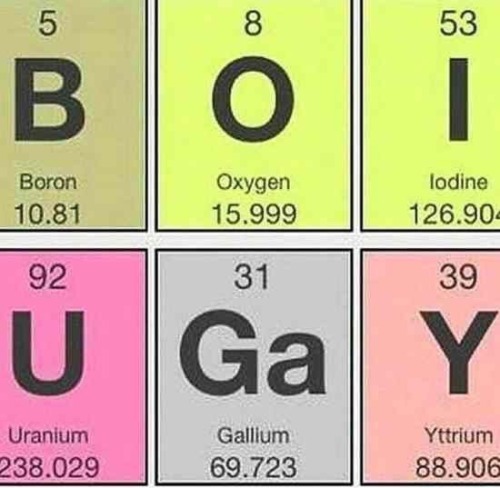
Yet another week begins, which means it’s time for METAL MONDAY! (Insert guitar solo here.) Today a profile a soft, silvery metal that looks a lot like mercury: gallium (Ga):
- Gallium destroys the structure of aluminum-zinc alloys or steel, by diffusing in between their crystalline boundaries. That’s science speak for “don’t take this on a place, it will eat through the fuselage.”
- The metal melts at about 302 K (29.7646 °C, 85.5763 °F) and boils more than eight times higher at 2673 K. According to Wikipedia (please fact check this for me!), this apparently gives gallium the greatest ratio between melting point and boiling point of any element.
- French chemist Paul-Émile Lecoq de Boisbaudran discovered the element in 1875. It’s said he named the element “gallia” from the Latin Gallia, meaning Gaul.
- Gallium is used in many alloys and also has useful applications in semiconductors.
(Image / Source Credit: Wikimedia Commons)
Post link
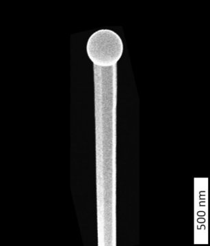
Array of nanowires gallium phosphide made with an electron microscope. Credit: Eindhoven University of Technology
Post link
An exotic material called gallium nitride (GaN) is poised to become the next semiconductor for power electronics, enabling much higher efficiency than silicon. In 2013, the Department of Energy (DOE) dedicated approximately half of a $140 million research institute for power electronics to GaN…
Scientists observe nanowires as they grow
X-ray experiments reveal exact details of self-catalyzed growth for the first time
At DESY’s X-ray source PETRA III, scientists have followed the growth of tiny wires of gallium arsenide live. Their observations reveal exact details of the growth process responsible for the evolving shape and crystal structure of the crystalline nanowires. The findings also provide new approaches to tailoring nanowires with desired properties for specific applications. The scientists, headed by Philipp Schroth of the University of Siegen and the Karlsruhe Institute of Technology (KIT), present their findings in the journal Nano Letters. The semiconductor gallium arsenide (GaAs) is widely used, for instance in infrared remote controls, the high-frequency components of mobile phones and for converting electrical signals into light for fibre optical transmission, as well as in solar panels for deployment in spacecraft.
To fabricate the wires, the scientists employed a procedure known as the self-catalysed Vapour-Liquid-Solid (VLS) method, in which tiny droplets of liquid gallium are first deposited on a silicon crystal at a temperature of around 600 degrees Celsius. Beams of gallium atoms and arsenic molecules are then directed at the wafer, where they are adsorpted and dissolve in the gallium droplets. After some time, the crystalline nanowires begin to form below the droplets, whereby the droplets are gradually pushed upwards. In this process, the gallium droplets act as catalysts for the longitudinal growth of the wires. “Although this process is already quite well established, it has not been possible until now to specifically control the crystal structure of the nanowires produced by it. To achieve this, we first need to understand the details of how the wires grow,” emphasises co-author Ludwig Feigl from KIT.
Post link
Going cubic halves the efficiency droop in InGaAlN light-emitting diodes
Today, it is widely accepted that the large Auger coefficient is the main cause for the large (~50%) efficiency droop in traditional hexagonal-phase InGaAlN LEDs. Yet, this explanation is inadequate to account for the low efficiency droop in gallium arsenide- and gallium phosphide-based LEDs, as those have similar Auger coefficients.
InIEEE Transactions on Electron Devices, Can Bayram, Jean-Pierre Leburton and Yi-Chia Tsai at the University of Illinois at Urbana-Champaign show that the coexistence of strong internal polarization and large carrier effective mass accounts for ~51% of the efficiency droop under high current densities in hexagonal-phase green InGaAlN LEDs (h-LEDs) compared to cubic-phase InGaAlN green LEDs (c-LEDs).
Post link
Fun with gallium


