#scanning electron microscopy
Researchers find whimsy at the nano scale
At extremely small scales, looks can be deceiving. While at first glance you might see lily pads floating on a tranquil pond, this image is actually a clever adaptation of a snapshot taken on a scanning electron microscope.
In reality, the green spots are only a few micrometers across—smaller than width of a human hair. They make up a surface coating that was developed to limit the transmission of SARS-CoV-2, the virus that causes COVID-19. The coating is composed of a silver-based material applied to a glass surface. The lotus flower, though, was some added artistic flair courtesy of image-editing software.
Mohsen Hosseini, Ph.D. candidate in chemical engineering, and William Ducker, professor of chemical engineering, recently won an award in the National Nanotechnology Coordinated Infrastructure (NNCI) image contest with this image. Both Hosseini and Ducker are affiliated with the Macromolecules Innovation Institute (MII).
Their win was in the category “most whimsical.”
Post link
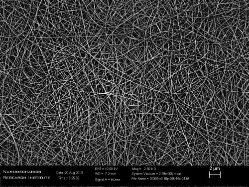
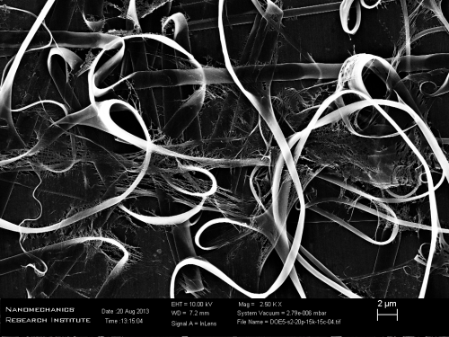
SEM imaging of our newly electrospun nanofibre composites. Fibre diameters from Sample 3 (images 2 and 4 here) have projected diameters of 40 - 100 nm, which are excellent results for this stage in the research.
The other images just look really, really cool, so I thought I’d share them as well!
Post link
I just wanted to let everyone know I’m doing two more days of ten posts each day, then going back to my usual five posts a day. If you’re not interested in seeing the images, go ahead and blacklist SEM or Scanning Electron Microscopy. If you like that sort of thing though I recommend simply searching Scanning Electron Microscopy (or Microscope) here on tumblr, checking out nanofabrication, an entire blog dedicated to SEM images, visiting lewisandquarks‘s blog (I’m reblogging quite a few but not all of their images and they seem to know a thing or two about SEMs), or going to ZEISS Microscopy’s flickr, or FEI‘s image gallery.
Nanorosesby Argonne National Laboratory
NanorosesBy Vilas G. Pol These tiny crystalline “roses” of europium oxycarbonate are formed under intense heat and pressure in a controlled system. Under certain conditions, they emit bright red light. Scientists are working to investigate the material’s luminescence intensity and decay time. Europium oxide, a related compound, has proven useful in lasers and high-density optical storage devices, and researchers hope to discover more about this unusual oxycarbonate compound and its potential applications. Previously published: Pol V.G. et al. Inorg. Chem. 2009, 48, 5569–5573
Post link
Materials Characterization: Scanning Electron Microscopy
One of the many instruments that uses electrons to view the surface of a material is the scanning electron microscope, or SEM. In order to achieve a higher resolution and greater magnification than is possible with ordinary light, scientists turned to electrons and the resolution of an SEM can approach a few nanometers. SEMs don’t actually snap a picture of the surface but rather provide the contrastthat produces an image. The resulting image, called a micrograph, is very similar to what you would expect if you could actually “see” the surface. SEM images are always monochrome but are often edited to produce false color images (sometimes similar to the real material, sometimes vastly different).
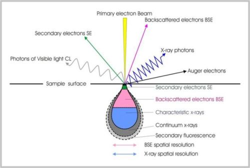
How though, do electrons produce an image? It all depends on how they react with the sample. An SEM contains a series of magnetic lenses that focus the beam of electrons similarly to how glass lenses focus light in an optical microscope. This beam of electrons then hits the surface of the sample and can undergo either inelasticorelastic scattering, resulting in the emission of electrons. It is these emitted electrons that are analyzed. Secondary electrons are low-energy electrons that are ejected from the specimen atoms by inelastic scattering. Backscattered electrons are high-energy electrons from the original electron beam that are reflected or back-scattered by elastic scattering.
Some of the most common methods for producing the electron beam itself are thermionic tungsten, LaB6, and hot and cold field emission.
Unlike an optical microscope, an SEM has a few sample requirements. For one, the material has to be vacuum compatible. For another, it helps to have a conducting material. If your material isn’t a conductor it must be coated with a thin conducting film (usually around ten nanometers) of carbon, gold, or some other metal.
Thanks to the fantastic images it can provide, the scanning electron microscope is one of the most widely used tools for materials characterization.
Post link
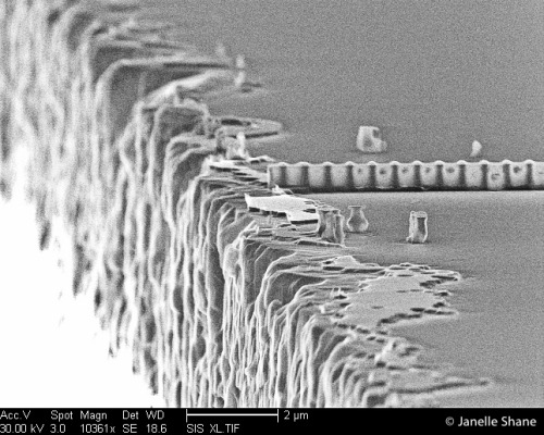
Standing at the edge of the world.
At microscopic scales, even a clean break isn’t very clean - this electron microscope picture is of the edge of a piece of glass, on which I had fabricated a long wall of semiconductor (the long columned wall you see at the middle right). I had zoomed in on this spot to make sure the wall went all the way to the edge of the glass. What I didn’t expect to see were these little guys clustered near the edge, seeming to look out over into the abyss. They were probably formed by little bits of debris (their little hats), that flew from the edge when it was cut. Since I made the nearby wall by etching away all of the semiconductor that wasn’t protected by a glassy wall-shaped mask, the same etching process left behind all the areas that were protected by the little debris hats. They’re small - if you stacked 200 of them on top of each other, they’d just about equal the thickness of a single human hair.
Post link
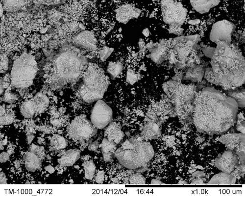
So this is a Scanning Electron Microscope (SEM) photo I took today of one of my samples of tungsten (VI) oxide, this is the sample marketed as <20 micrometers (10^-6 m ) in diameter. As you can see there are some particles that at bigger than this which tells you that suppliers can’t be trusted with what they say…
But It also shows that the particles are not regular shapes which can effect the stability of the emulsions formed with them. This was what the powder looks like as it has been supplied, if I was to sonicate this the particles should be much smaller on average
I just thought it was a really nice picture and there you go
Post link
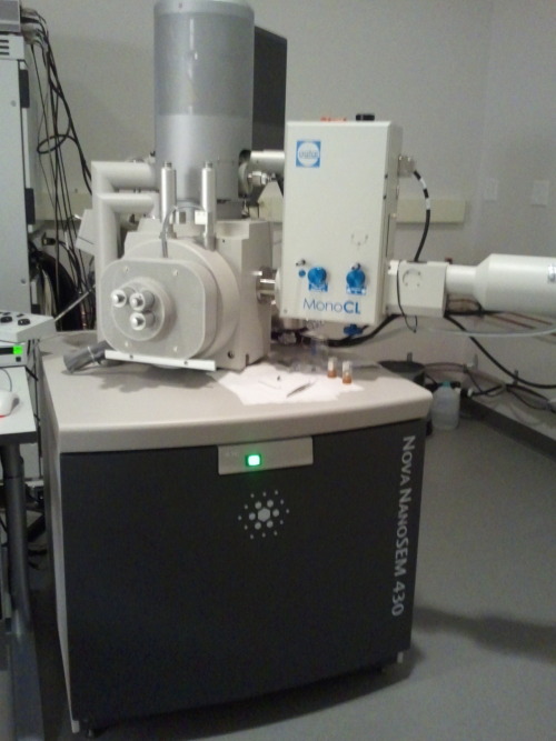
Behold, SEM. http://en.wikipedia.org/wiki/Scanning_electron_microscope Pretty sweet stuff if you ever get to use one
Post link
False-colour electron microscope image of the silicon nanoelectronic device which contains the phosphorus atom used for the demonstration of quantum entanglement. Credit: University of New South Wales
Post link
Scientists observe nanowires as they grow
X-ray experiments reveal exact details of self-catalyzed growth for the first time
At DESY’s X-ray source PETRA III, scientists have followed the growth of tiny wires of gallium arsenide live. Their observations reveal exact details of the growth process responsible for the evolving shape and crystal structure of the crystalline nanowires. The findings also provide new approaches to tailoring nanowires with desired properties for specific applications. The scientists, headed by Philipp Schroth of the University of Siegen and the Karlsruhe Institute of Technology (KIT), present their findings in the journal Nano Letters. The semiconductor gallium arsenide (GaAs) is widely used, for instance in infrared remote controls, the high-frequency components of mobile phones and for converting electrical signals into light for fibre optical transmission, as well as in solar panels for deployment in spacecraft.
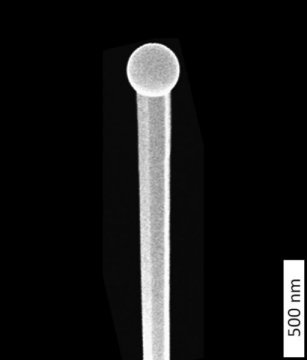
To fabricate the wires, the scientists employed a procedure known as the self-catalysed Vapour-Liquid-Solid (VLS) method, in which tiny droplets of liquid gallium are first deposited on a silicon crystal at a temperature of around 600 degrees Celsius. Beams of gallium atoms and arsenic molecules are then directed at the wafer, where they are adsorpted and dissolve in the gallium droplets. After some time, the crystalline nanowires begin to form below the droplets, whereby the droplets are gradually pushed upwards. In this process, the gallium droplets act as catalysts for the longitudinal growth of the wires. “Although this process is already quite well established, it has not been possible until now to specifically control the crystal structure of the nanowires produced by it. To achieve this, we first need to understand the details of how the wires grow,” emphasises co-author Ludwig Feigl from KIT.
Post link
External surface (Left) and Internal surface (Right) of blow-moulded HDPE
System: High density polyethylene (HDPE)
[…]
Processing: A ‘parison’ (tube) is continuously extruded into a mould which periodically closes together with a knife, to cut suitable lengths which are then expanded to fill the mould
Applications: Blow moulding is a continuous process used in the manufacture of bottles as well as sheets, bags, and tubes.
Sample preparation: The specimen has been sputter-coated with gold, to give a conducting surface
Technique: Scanning electron microscopy (SEM)
[…]
Further information [External surface]: The surface shows periodic ridges at right angles to the flow direction. These are indicative of flow instability and a periodic slipping of the melt at the die wall. It also shows surface scratches which are typical of polymer surfaces. Hard abrasive particles, dragged across the surface, have displaced material to form grooves and ridges.
Further information [Internal surface]: The surface shows ~5 micron periodic ridges which are indicative of flow instability and a periodic slipping of the melt at the die wall. On a finer scale are catspaws of submicron polymer, drawn up by the 'wind’ in the blowing process.
Contributor: J A Curran
Organisation: Department of Materials Science and Metallurgy, University of Cambridge
Post link
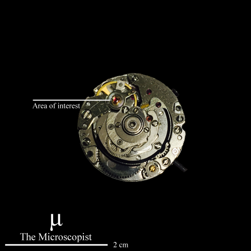
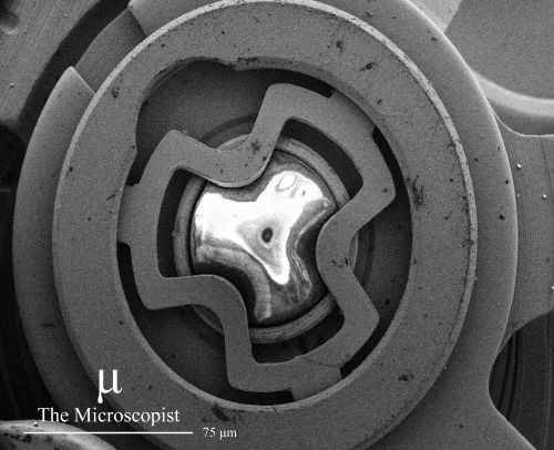
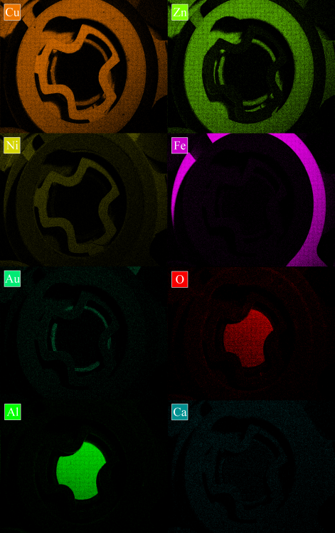
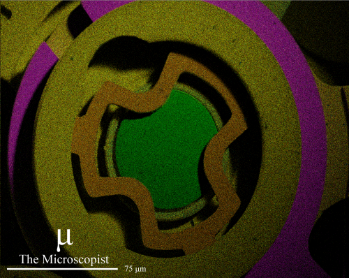
Optical and scanning electron microscope images, as well as elemental maps of a gear in a watch.
Post link


