#nanowires
A pathway to high-quality ZnSe quantum wires
One-dimensional semiconductor nanowires with strong quantum confinement effect—quantum wires (QWs)—are of great interest for applications in advanced optoelectronics and photochemical conversions. Beyond the state-of-the-art Cd-containing ones, ZnSe QWs, as a representative heavy-metal-free semiconductor, have shown the utmost potential for next-generation environmental-friendly applications.
Unfortunately, ZnSe nanowires produced thus far are largely limited to the strong quantum confinement regime with near-violet-light absorption or to the bulk regime with undiscernible exciton features. Simultaneous, on-demand, and high-precision manipulations on their radial and axial sizes—that allows strong quantum confinement in the blue-light region—has so far been challenging, which substantially impedes their further applications.
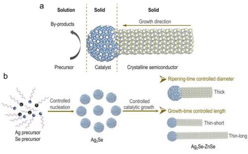
In a new article published in the National Science Review, a research team led by professor YU Shuhong at University of Science and Technology of China (USTC) has reported the on-demand synthesis of high-quality, blue-light-active ZnSe QWs by developing a flexible synthetic approach—a two-step catalytic growth strategy that enables independent, high-precision, and wide-range controls over the diameter and length of ZnSe QWs. In this way, they bridge the gap between prior magic-sized ZnSe QWs and bulk-like ZnSe nanowires.
Post link
Solar Nanowire-Nanotube Purification Filter Offers Easy Access To Clean Drinking Water
Even today, clean water is a privilege for many people across the world. According to the World Health Organization (WHO), at least 1.8 billion people consume water contaminated with feces, and by 2040, a large portion of the world will endure water stress because of insufficient resources of drinking water. Meanwhile, the United Nations Children’s Fund (UNICEF), around 1,800 children die every day from diarrhea because of unsafe water supply, which causes diseases like cholera.
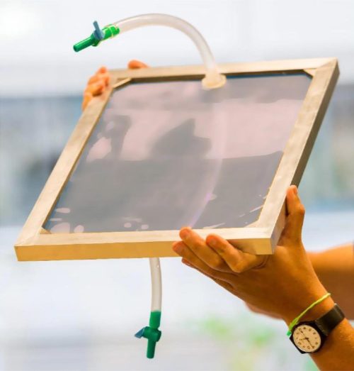
It has become imperative then that we develop efficient and cost-efficient ways to decontaminate water. And that is exactly what a team of scientists led by László Forró at EPFL have accomplished, with a new water purification filter that combines titanium dioxide (TiO2) nanowires and carbon nanotubes powered by nothing but sunlight.
The scientists first show that the TiO2nanowires by themselves can efficiently purify water in the presence of sunlight. But interweaving the nanowires with carbon nanotubes forms a composite material that adds an extra layer of decontamination by pasteurizing the water – killing off human pathogens such as bacteria and large viruses.
Post link
Digitally programmable perovskite nanowire-block copolymer composites
One-dimensional nanomaterials with highly anisotropicoptoelectronic properties can be used within energy harvesting applications, flexible electronics and biomedical imaging devices. In materials science and nanotechnology, 3-D patterning methods can be used to precisely assemble nanowires with locally controlled composition and orientation to allow new optoelectronic device designs. In a recent report, Nanjia Zhou and an interdisciplinary research team at the Harvard University, Wyss Institute of Biologically Inspired Engineering, Lawrence Berkeley National Laboratory and the Kavli Energy Nanoscience Institute developed and 3-D printed nanocomposite inks composed of brightly emitting colloidal cesium lead halide perovskite (CsPbX3, where X= Cl, Br, or I) nanowires.
They suspended the bright nanowires in a polystyrene-polyisoprene-polystyrene block copolymer matrix and defined the nanowire alignment using a programmed print path. The scientist produced optical nanocomposites that exhibited highly polarized absorption and emission properties. To highlight the versatility of the technique they produced several devices, including optical storage, encryption, sensing and full color displays. The work is now published on Science Advances.
Post link
Scientists observe nanowires as they grow
X-ray experiments reveal exact details of self-catalyzed growth for the first time
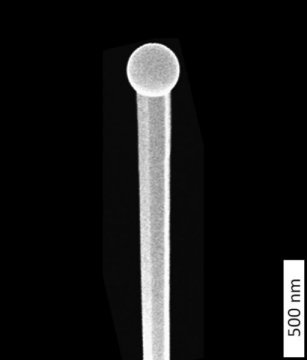
At DESY’s X-ray source PETRA III, scientists have followed the growth of tiny wires of gallium arsenide live. Their observations reveal exact details of the growth process responsible for the evolving shape and crystal structure of the crystalline nanowires. The findings also provide new approaches to tailoring nanowires with desired properties for specific applications. The scientists, headed by Philipp Schroth of the University of Siegen and the Karlsruhe Institute of Technology (KIT), present their findings in the journal Nano Letters. The semiconductor gallium arsenide (GaAs) is widely used, for instance in infrared remote controls, the high-frequency components of mobile phones and for converting electrical signals into light for fibre optical transmission, as well as in solar panels for deployment in spacecraft.
To fabricate the wires, the scientists employed a procedure known as the self-catalysed Vapour-Liquid-Solid (VLS) method, in which tiny droplets of liquid gallium are first deposited on a silicon crystal at a temperature of around 600 degrees Celsius. Beams of gallium atoms and arsenic molecules are then directed at the wafer, where they are adsorpted and dissolve in the gallium droplets. After some time, the crystalline nanowires begin to form below the droplets, whereby the droplets are gradually pushed upwards. In this process, the gallium droplets act as catalysts for the longitudinal growth of the wires. “Although this process is already quite well established, it has not been possible until now to specifically control the crystal structure of the nanowires produced by it. To achieve this, we first need to understand the details of how the wires grow,” emphasises co-author Ludwig Feigl from KIT.
Post link
Printed electronics breakthrough could lead to flexible electronics revolution
A new form of electronics manufacturing which embeds silicon nanowires into flexible surfaces could lead to radical new forms of bendable electronics, scientists say.
In a new paper published today in the journal Microsystems and Nanoengineering, engineers from the University of Glasgow describe how they have for the first time been able to affordably ‘print’ high-mobility semiconductor nanowires onto flexible surfaces to develop high-performance ultra-thin electronic layers.
Those surfaces, which can be bent, flexed and twisted, could lay the foundations for a wide range of applications including video screens, improved health monitoring devices, implantable devices and synthetic skin for prosthetics.
The paper is the latest development from the University of Glasgow’s Bendable Electronics and Sensing Technologies (BEST) research group, led by Professor Ravinder Dahiya.
Post link


