#quantum dots
Suppressing the Auger recombination process in quantum dots
A Quantum Dot (QD) is a nanometer-sized semiconductor nanocrystal that has unique optical properties such as the ability to emit light in the range of optical frequencies depending on its size. QDs have already been applied to practical optoelectronic applications including light-emitting displays, solar cells, photodetectors, and lasers.
In general, QDs have two distinct energy bands in which electrons can exist. They are the so-called “valence band” where electrons are fully occupied and the “conduction band” where electrons are empty, respectively. The gap between these two bands is called the “band gap,” where electrons cannot exist. Upon photoexcitation by light with higher energy than the band gap, electrons within the valence band can be excited and jump into the conduction band. A vacancy formed in the valence band after this process is called a “hole,” which is defined as a carrier having a positive charge.
A hole usually pairs with an electron in the conduction band and forms a quasi-particle called an “exciton” that is bound via Coulomb interaction. After formation, the exciton can recombine spontaneously and emit light with the same energy as the band gap. The most important parameter in this process is the “transition dipole moment,” which is an electric dipole moment associated with the transition between the two states. Typically, the larger this quantity, the greater the recombinationrate.
Post link
Ultrafast imaging of terahertz electric waveforms using quantum dots
Microscopic electric fields govern a remarkable variety of phenomena in condensed matter and their ultrafast evolutions drive plasmonics, phononics and highspeed nanoelectronics. Access to high-frequency electric waveforms is of crucial importance to diverse disciplines in nanoscience and technology, yet, microscopic measurements are still severely limited.
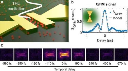
In a new paper published in Light: Science & Applications, a team of scientists, led by Prof. Georg Herink from the University of Bayreuth, Germany, and co-workers from the University of Melbourne, Australia, has introduced a new THz microscope for imaging ultrafast electric waveforms encoded in the visible luminescence of nanocrystal probes. Strong electric fields modulate the emission yield of nanocrystals and enable the detection of THz near-field waveforms by microscopy of visible photons in the far-field.
The researchers generated ultrafast electric fields inside gold structures using intense Terahertz pulses. A layer of semiconductor nanocrystals covering the samples is excited by ultrashort visible pulses and shows modulated visible emission depending on the momentary local THz electric field. Fundamentally, this probing of electric fields via luminescence yield is enabled by the quantum-confined Stark effect in quantum dots, generating the contrast mechanism of the scheme termed Quantum-Probe Field Microscopy (QFIM). While scanning the temporal delay between THz excitation and optical pulses, an optical fluorescence microscope captures snapshots of the modulated local emission and generates movies of the local fieldevolution.
Post link
Development of a transparent and flexible ultra-thin memory device
A two-dimensional (2D) nanomaterial-based flexible memory device is a critical element in the next-generation wearable market because it plays a crucial role in data storage, processing, and communication. An ultra-thin memory device materialized with a 2D nanomaterial of several nanometers (nm) can significantly increase the memory density, leading to the development of a flexible resistance-variable memory with the implementation of a 2D nanomaterial. However, memories using conventional 2D nanomaterials have limitations owing to the weak carrier trapping characteristics of the nanomaterials.
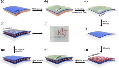
At the Institute of Advanced Composite Materials, Korea Institute of Science and Technology (KIST, President Yoon, Seok-Jin), a research team led by Dr. Dong-Ick Son announced the development of a transparent and flexible memory device based on a heterogeneous low-dimensional ultra-thin nanostructure. To this end, monolayered zero-dimensional (0D) quantum dots were formed and sandwiched between two insulating 2D hexagonal boron nitride (h-BN) ultra-thin nanomaterialstructures.
The research team materialized a device that could become a next-generation memory candidate by introducing 0D quantum dots with excellent quantum limiting properties into the active layer, controlling carriers in 2D nanomaterial. Based on this, 0D quantum dots were shaped in a vertically stacked composite structure that was sandwiched between 2D hexagonal h-BN nanomaterials to produce a transparent and flexible device. Therefore, the developed device maintains above 80% transparency and memory function even when bent.
Post link
Researchers developing 2-D materials similar to graphene
Chemists are working to synthesize the next generation of super materials for high-performance electronics, solar cells, photodetectors and quantum computers. While they have made progress with compound materials, they have not yet succeeded in developing unaltered or “freestanding” materials for such devices, according to a review published in the journal Science and Technology of Advanced Materials.
Graphene is a carbon material derived from graphite, the same type of material found in pencils, but it is arranged in a one-atom-thin honeycomb lattice. Discovered in 2004, graphene’s two-dimensional arrangement gives it “extraordinary” properties, including extreme strength and “marvelously high” electron conductivity.
However, the tight lattice lacks a semiconducting bandgap, which is essential for electronic devices. Therefore, scientists have been hunting for alternative materials that have bandgaps, but still have a graphene-like structure.
Much focus has been placed on graphene quantum dots, which are small segments of graphene, about 10 to 100 nm carbon hexagons across and less than 30 atomic sheets thick. To make the dots behave more like 2-D graphene, research teams have added other molecules to change the structure and function of the material.
Post link
Researchers have developed a new method for growing ‘hybrid’ crystals at the nanoscale, in which quantum dots – essentially nanoscale semiconductors – of different materials can be sequentially incorporated into a host nanowire with perfect junctions between the components. Images recorded in …

Шевели мозгами.
http://4pda.ru/2014/12/29/194105/
Канадческая клоповница.
http://www.nat-geo.ru/article/5737-krov-biologa-pomogla-izobresti-lovushku-dlya-klopov/
Nokia rise.
http://androidinsider.ru/smartfony/nokia-c1-novyiy-android-smartfon.html
Мемристор всё.
http://www.3dnews.ru/907207/
Тебе там датчиками намазано?
http://www.3dnews.ru/907148/
Анжелика, откуда звук?
http://www.3dnews.ru/907189/
Метрическая система в штатах?
http://www.vox.com/2014/5/29/5758542/time-for-the-US-to-use-the-metric-system
Квантовые точки.
http://www.3dnews.ru/907084/
https://ru.wikipedia.org/wiki/%D0%9A%D0%B2%D0%B0%D0%BD%D1%82%D0%BE%D0%B2%D0%B0%D1%8F_%D1%82%D0%BE%D1%87%D0%BA%D0%B0


