#boron nitride
Trapping gases better with boron nitride ‘nanopores’
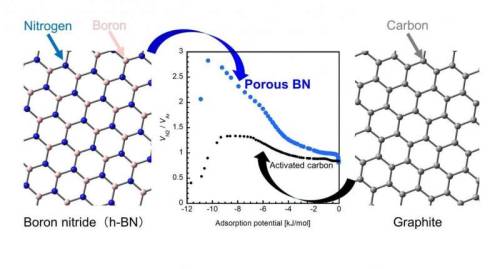
What is common between a technology for storing energy in a solar cell and that for water purification? They both rely on the use of porous materials, or more specifically, 'nanoporous’ materials that can trap gas molecules within narrow spaces on their surface, called pores, which are only nanometers (one-billionth of a meter) in size. In the parlance of chemistry, the phenomenon is known as adsorption and has played an important role in the synthesis of porous materials of different compositions, pore sizes, and even pore geometries.
Traditionally, activated carbon (AC, or a porous form of carbon) has been a popular adsorbent for practical applications owing to its higher capacity of adsorption than that of other porous materials. Lately, however, porous boron nitride (p-BN) has emerged as a promising alternative because of its impressive performance, as highlighted by a recent study claiming that p-BN can adsorb a relatively large amount of carbon dioxide at room temperature.
Now, a group of scientists from Okayama University and Nagasaki University, Japan, has put this claim to the test in their latest study, where they examined the adsorbing characteristics of p-BN in detail. “A BN unit and two carbon atoms (i.e., CC) both have the same number of electrons and similar structures, but their interaction with gas molecules are different due to the atomically heterogeneous nature of BN. Despite this, there has been very little research on BN materials. In our study, we wanted to see if BN has specific adsorption properties that cannot be observed in carbon materials,” explains Dr. Takahiro Ohkubo from Okayama University, who led this study published in the journal RSC Advances.
Post link
Curbing the flammability of epoxy resin
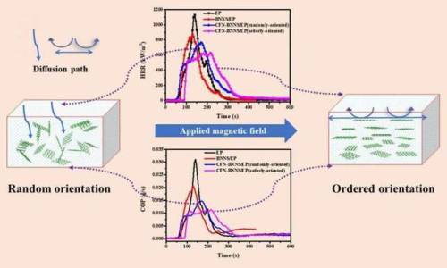
In a paper to be published in a forthcoming issue of Nano, a team of researchers from Henan University have investigated the flame retardant performance of epoxy resin using a boron nitride nanosheet decorated with cobalt ferrite nanoparticles.
Polymers are widely used in our daily lives due to good physical and chemical stability, corrosion resistance and other superior properties. However, most polymers, due to their organic nature, are inherently flammable which is a potential threat to the safety of human life and property. In order to avoid or reduce the flammability of polymers, it is a good strategy to add flame retardants to the polymers.
Among them, two-dimensional (2-D) layered inorganic nanomateirals (nanosheets), represented by graphene oxide,molybdenum disulfide, and boron nitride nanosheets (BNNS), exhibit excellent flame retardant performance due to their good physical barrier effects. However, the flame retardance is not enough in the use of such 2-D inorganic flame retardants alone, and in particular, the ability to suppress toxic gases and smoke is weak.
Post link
A graphene superconductor that plays more than one tune: Researchers at Berkeley Lab have developed a tiny toolkit for scientists to study exotic quantum physics
Researchers at the U.S. Department of Energy’s Lawrence Berkeley National Laboratory (Berkeley Lab) have developed a graphene device that’s thinner than a human hair but has a depth of special traits. It easily switches from a superconducting material that conducts electricity without losing any energy, to an insulator that resists the flow of electric current, and back again to a superconductor - all with a simple flip of a switch. Their findings were reported today in the journal Nature.
[…]
“Usually, when someone wants to study how electrons interact with each other in a superconducting quantum phase versus an insulating phase, they would need to look at different materials. With our system, you can study both the superconductivity phase and the insulating phase in one place,” said Guorui Chen, the study’s lead author and a postdoctoral researcher in the lab of Feng Wang, who led the study. Wang, a faculty scientist in Berkeley Lab’s Materials Sciences Division, is also a UC Berkeley physics professor.
Post link
Development of a transparent and flexible ultra-thin memory device
A two-dimensional (2D) nanomaterial-based flexible memory device is a critical element in the next-generation wearable market because it plays a crucial role in data storage, processing, and communication. An ultra-thin memory device materialized with a 2D nanomaterial of several nanometers (nm) can significantly increase the memory density, leading to the development of a flexible resistance-variable memory with the implementation of a 2D nanomaterial. However, memories using conventional 2D nanomaterials have limitations owing to the weak carrier trapping characteristics of the nanomaterials.
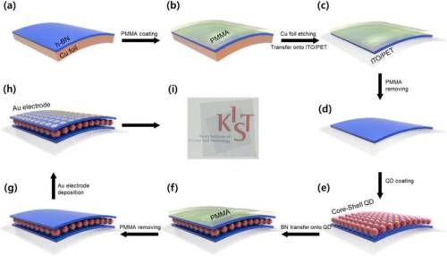
At the Institute of Advanced Composite Materials, Korea Institute of Science and Technology (KIST, President Yoon, Seok-Jin), a research team led by Dr. Dong-Ick Son announced the development of a transparent and flexible memory device based on a heterogeneous low-dimensional ultra-thin nanostructure. To this end, monolayered zero-dimensional (0D) quantum dots were formed and sandwiched between two insulating 2D hexagonal boron nitride (h-BN) ultra-thin nanomaterialstructures.
The research team materialized a device that could become a next-generation memory candidate by introducing 0D quantum dots with excellent quantum limiting properties into the active layer, controlling carriers in 2D nanomaterial. Based on this, 0D quantum dots were shaped in a vertically stacked composite structure that was sandwiched between 2D hexagonal h-BN nanomaterials to produce a transparent and flexible device. Therefore, the developed device maintains above 80% transparency and memory function even when bent.
Post link
Hexagonal boron nitride semiconductors enable cost-effective detection of neutron signals
One of the most critical issues the United States faces today is preventing terrorists from smuggling nuclear weapons into its ports. To this end, the U.S. Security and Accountability for Every Port Act mandates that all overseas cargo containers be scanned for possible nuclear materials or weapons.
Detecting neutron signals is an effective method to identify nuclear weapons and special nuclear materials. Helium-3 gas is used within detectors deployed in ports for this purpose.
The catch? While helium-3 gas works well for neutron detection, it’s extremely rare on Earth. Intense demand for helium-3 gas detectors has nearly depleted the supply, most of which was generated during the period of nuclear weapons production during the past 50 years. It isn’t easy to reproduce, and the scarcity of helium-3 gas has caused its cost to skyrocket recently – making it impossible to deploy enough neutron detectors to fulfill the requirement to scan all incoming overseas cargo containers.
Helium-4 is a more abundant form of helium gas, which is much less expensive, but can’t be used for neutron detection because it doesn’t interact with neutrons.
A tiny instrument to measure the faintest magnetic fields
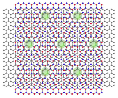
Physicists at the University of Basel have developed a minuscule instrument able to detect extremely faint magnetic fields. At the heart of the superconducting quantum interference device are two atomically thin layers of graphene, which the researchers combined with boron nitride. Instruments like this one have applications in areas such as medicine, besides being used to research new materials.
To measure very small magnetic fields, researchers often use superconducting quantum interference devices, or SQUIDs. In medicine, their uses include monitoring brain or heart activity, for example, while in the earth sciences researchers use SQUIDs to characterize the composition of rocks or detect groundwater flows. The devices also have a broad range of uses in other applied fields and basic research.
The team led by Professor Christian Schönenberger of the University of Basel’s Department of Physics and the Swiss Nanoscience Institute has now succeeded in creating one of the smallest SQUIDs ever built. The researchers described their achievement in the scientific journal Nano Letters.


