#electrons
Suppressing the Auger recombination process in quantum dots
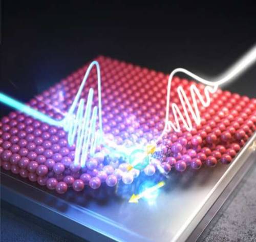
A Quantum Dot (QD) is a nanometer-sized semiconductor nanocrystal that has unique optical properties such as the ability to emit light in the range of optical frequencies depending on its size. QDs have already been applied to practical optoelectronic applications including light-emitting displays, solar cells, photodetectors, and lasers.
In general, QDs have two distinct energy bands in which electrons can exist. They are the so-called “valence band” where electrons are fully occupied and the “conduction band” where electrons are empty, respectively. The gap between these two bands is called the “band gap,” where electrons cannot exist. Upon photoexcitation by light with higher energy than the band gap, electrons within the valence band can be excited and jump into the conduction band. A vacancy formed in the valence band after this process is called a “hole,” which is defined as a carrier having a positive charge.
A hole usually pairs with an electron in the conduction band and forms a quasi-particle called an “exciton” that is bound via Coulomb interaction. After formation, the exciton can recombine spontaneously and emit light with the same energy as the band gap. The most important parameter in this process is the “transition dipole moment,” which is an electric dipole moment associated with the transition between the two states. Typically, the larger this quantity, the greater the recombinationrate.
Post link
Electrons go with the flow
You turn on a switch and the light switches on because electricity ‘flows’. The usual perception is that this is like opening a faucet and the water starts to flow. But this analogy is misleading. The flow of water is determined by the theory of hydrodynamics, where the behavior of the fluid requires no knowledge of the movements of individual molecules.
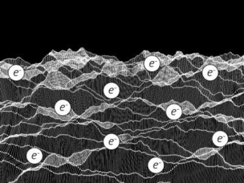
However, electric currents in solids are formed by electrons. In metals, the electrons do not collide with each other, but they scatter with lattice defects. In conventional materials, the movement of electrons is therefore more akin to the motion of balls in a pinball machine.
Hydrodynamic electron flow can only be observed in high-purity quantum materials. An international team of members from the IBM Research Laboratory Zurich, the University of Hamburg and the Max Planck Institute for Chemical Physics of Solids has now found signatures of electron hydrodynamics in the semimetal tungsten diphosphide. The results were published in the journal Nature Communications. On closer inspection, it could be shown that the hydrodynamic behavior of the electrons is rooted in the strongly interacting quantum nature of the electron system.
Post link
Ultrafast optical fiber-based electron gun to reveal atomic motions
One of the most enduring “Holy Grail” experiments in science has been attempts to directly observe atomic motions during structural changes. This prospect underpins the entire field of chemistry because a chemical process occurs during a transition state—the point of no return separating the reactant configuration from the product configuration.
What does that transition state look like and, given the enormous number of different possible nuclear configurations, how does a system even find a way to make it happen?
Now in the journal Applied Physics Letters, researchers at the Max Planck Institute for the Structure and Dynamics of Matter are reporting “ultrabright” electron sources with sufficient brightness to literally light up atomic motions in real time—at a time scale of 100 femtoseconds, making these sources particularly relevant to chemistry because atomic motions occur in that window of time.
After seeing the first atomic movies of phase transitions in bulk thin films using high-energy (100 kilovolt) electron bunches, the researchers wondered if they could achieve atomic resolution of surface reactions—occurring within the first few monolayers of materials—to gain a better understanding of surface catalysis.
Post link
Controlling traffic on the electron highway—researching graphene
On an otherwise normal day in the lab, Eva Andrei didn’t expect to make a major discovery. Andrei, a physics professor at Rutgers University, was using graphite – the material in pencils – to calibrate a scanning tunneling microscope. As part of the process, she turned on a very powerful magnetic field. When she looked up to see the material’s electronic spectrum, she was astonished. “We saw huge, beautiful peaks up there, just incredible. And they didn’t make any sense,” she recalled.
Remembering a lecture she’d recently attended, she realized the graphite had separated out into sheets just one atom thick. This material, known as graphene, has bizarre electronic properties. But even for graphene, the spectrum she saw was strange. In fact, no one had ever seen anything like it before. As Andrei described it, her colleague “went berserk in the corridor and just yelled ‘Graphene!’” Andrei had made a serendipitous discovery – a new electric phenomenon.
This was neither the first nor last time that electrons’ movement in graphene would surprise and elate scientists. One of the most impressive things about graphene is how fast electrons move through it. They travel through it more than 100 times faster than they do through the silicon used to make computer chips. In theory, this suggests that manufacturers could use graphene to make superfast transistors for faster, thinner, more powerful touch-screens, electronics, and solar cells.
Post link
Materials Characterization: Scanning Electron Microscopy
One of the many instruments that uses electrons to view the surface of a material is the scanning electron microscope, or SEM. In order to achieve a higher resolution and greater magnification than is possible with ordinary light, scientists turned to electrons and the resolution of an SEM can approach a few nanometers. SEMs don’t actually snap a picture of the surface but rather provide the contrastthat produces an image. The resulting image, called a micrograph, is very similar to what you would expect if you could actually “see” the surface. SEM images are always monochrome but are often edited to produce false color images (sometimes similar to the real material, sometimes vastly different).
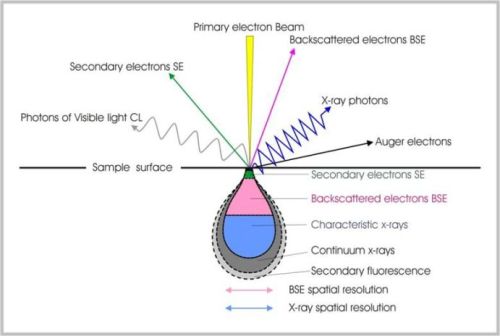
How though, do electrons produce an image? It all depends on how they react with the sample. An SEM contains a series of magnetic lenses that focus the beam of electrons similarly to how glass lenses focus light in an optical microscope. This beam of electrons then hits the surface of the sample and can undergo either inelasticorelastic scattering, resulting in the emission of electrons. It is these emitted electrons that are analyzed. Secondary electrons are low-energy electrons that are ejected from the specimen atoms by inelastic scattering. Backscattered electrons are high-energy electrons from the original electron beam that are reflected or back-scattered by elastic scattering.
Some of the most common methods for producing the electron beam itself are thermionic tungsten, LaB6, and hot and cold field emission.
Unlike an optical microscope, an SEM has a few sample requirements. For one, the material has to be vacuum compatible. For another, it helps to have a conducting material. If your material isn’t a conductor it must be coated with a thin conducting film (usually around ten nanometers) of carbon, gold, or some other metal.
Thanks to the fantastic images it can provide, the scanning electron microscope is one of the most widely used tools for materials characterization.
Post link
Researchers observe electrons zipping around in crystals
The end of the silicon age has begun. As computer chips approach the physical limits of miniaturization and power-hungry processors drive up energy costs, scientists are looking to a new crop of exotic materials that could foster a new generation of computing devices that promise to push performance to new heights while skimping on energy consumption.
Unlike current silicon-based electronics, which shed most of the energy they consume as waste heat, the future is all about low-power computing. Known as spintronics, this technology relies on a quantum physical property of electrons – up or down spin – to process and store information, rather than moving them around with electricity as conventional computing does.
On the quest to making spintronic devices a reality, scientists at the University of Arizona are studying an exotic crop of materials known as transition metal dichalcogenides, or TMDs. TMDs have exciting properties lending themselves to new ways of processing and storing information and could provide the basis of future transistors and photovoltaics – and potentially even offer an avenue toward quantum computing.
For example, current silicon-based solar cells convert realistically only about 25 percent of sunlight into electricity, so efficiency is an issue, says Calley Eads, a fifth-year doctoral student in the UA’s Department of Chemistry and Biochemistry who studies some of the properties of these new materials. “There could be a huge improvement there to harvest energy, and these materials could potentially do this,” she says.
Post link
Fast-moving electrons create current in organic solar cells
Researchers at Purdue University have identified the mechanism that allows organic solar cells to create a charge, solving a longstanding puzzle in physics, according to a paper published Friday (Jan. 12) in the journal Science Advances.
Organic solar cells are built with soft molecules, while inorganic solar cells, often silicon-based, are built with more rigid materials. Silicon cells currently dominate the industry, but they’re expensive and stiff, while organic cells have the potential to be light, flexible and cheap. The drawback is that creating an electric current in organic cells is much more difficult.
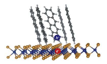
To create an electrical current, two particles, one with a negative charge (electron) and one with a positive charge (electron-hole), must separate despite being bound tightly together. These two particles, which together form an exciton, usually require a manmade interface to separate them. The interface draws the electron through an electron acceptor and leaves the hole behind. Even with the interface in place, the electron and hole are still attracted to each other – there’s another mechanism that helps them separate.
“We discovered that this type of electron-hole interface is not one single static state. The electron and the hole can be far apart or close together, and the farther apart they are, the more likely they are to separate,” said Libai Huang, an assistant professor of chemistry in Purdue’s College of Science, who led the research. “When they’re far apart, they’re actually very mobile, and they can move pretty fast. We think that this kind of fast motion between the positive and negative charge is what’s driving separation at these interfaces.”
Post link
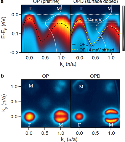
Enhanced electron doping on iron superconductors discovered
The Institute for Basic Science research team headed by the associate director of CCES, KIM Chang Young, presented the possibility of unifying theories to explain the working mechanism of iron- based superconductors.
Their research was published in Nature Materials on August 16th. Superconductors are a relatively new concept; they were brought to prominence in the late 80’s when two Nobel Prize winners discovered a new superconducting material. The basic principle of superconductivity arises when a superconducting material is cooled to a fairly low critical temperature allowing an electric current to flow without resistance.
Building on a Nobel Prize
The Nobel Prize winners reported their superconducting material - oxides which contain copper and rare earth metals - becomes a superconducting material below -250° Celsius, higher than the previous temperature of -269° Celsius. This led to a boom in developing similar materials for commercial use. Today’s research has moved on greatly; oxides are replaced with iron-based superconductors which are cheaper to mass produce and also permit a current to flow unabated. To understand the working mechanism of iron-based superconductors scientists have to significantly raise the transition temperatures to source the reason for the increase. Many researchers initially work on the assumption that the nesting effect is a dominant factor, especially in the case of pnictide superconductors {PSD}. Later, scientists discovered another type of superconductor, chalogenide superconductors {CSD}. Since it turned out that CSD is not subject to the nesting effect, the discovery of CSD generated controversy on the mechanism of their superconductivity. The nesting effect states when the surface temperature is increased, electrons become unstable thereby altering their properties both electrically and magnetically, allowing conductors to turn into superconductors.
Post link
After 15 Years of Research, Scientists Reveal the Fourth Signature of the Superconducting Transitions
The results cap 15 years of detective work aimed at understanding how these materials transition into a superconducting state where they can conduct electricity with no loss.
Researchers were ecstatic 35 years ago when a novel and exciting new class of superconducting materials was found.
These copper oxides or cuprates, like other superconductors, conducted electricity without resistance or loss when chilled below a specific degree – but at substantially larger temperatures than scientists had expected. This increased the possibility of having them to work at temperatures near to room temperature for perfectly efficient power lines and other uses.
Research quickly confirmed that they demonstrated two additional classic characteristics of the transition to a superconducting state. The material expelled magnetic fields as superconductivity occurred, allowing a magnet placed on a chunk of the material to hover above the surface. And during the transition, their heat capacity – the amount of heat required to raise their temperature by a certain amount – displayed a notable abnormality.
Post link
A single neuron in isolation cannot be said to possess memory, feelings, or consciousness. However, group many neurons together and the type of advanced information processing that takes place in the human brain suddenly appears. This suggests that perhaps each level in the micro-macro hierarchy…
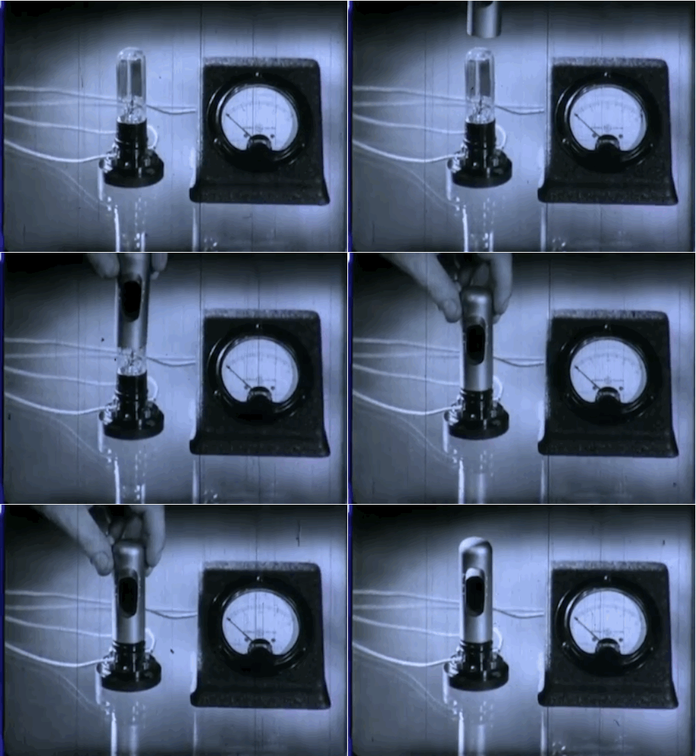
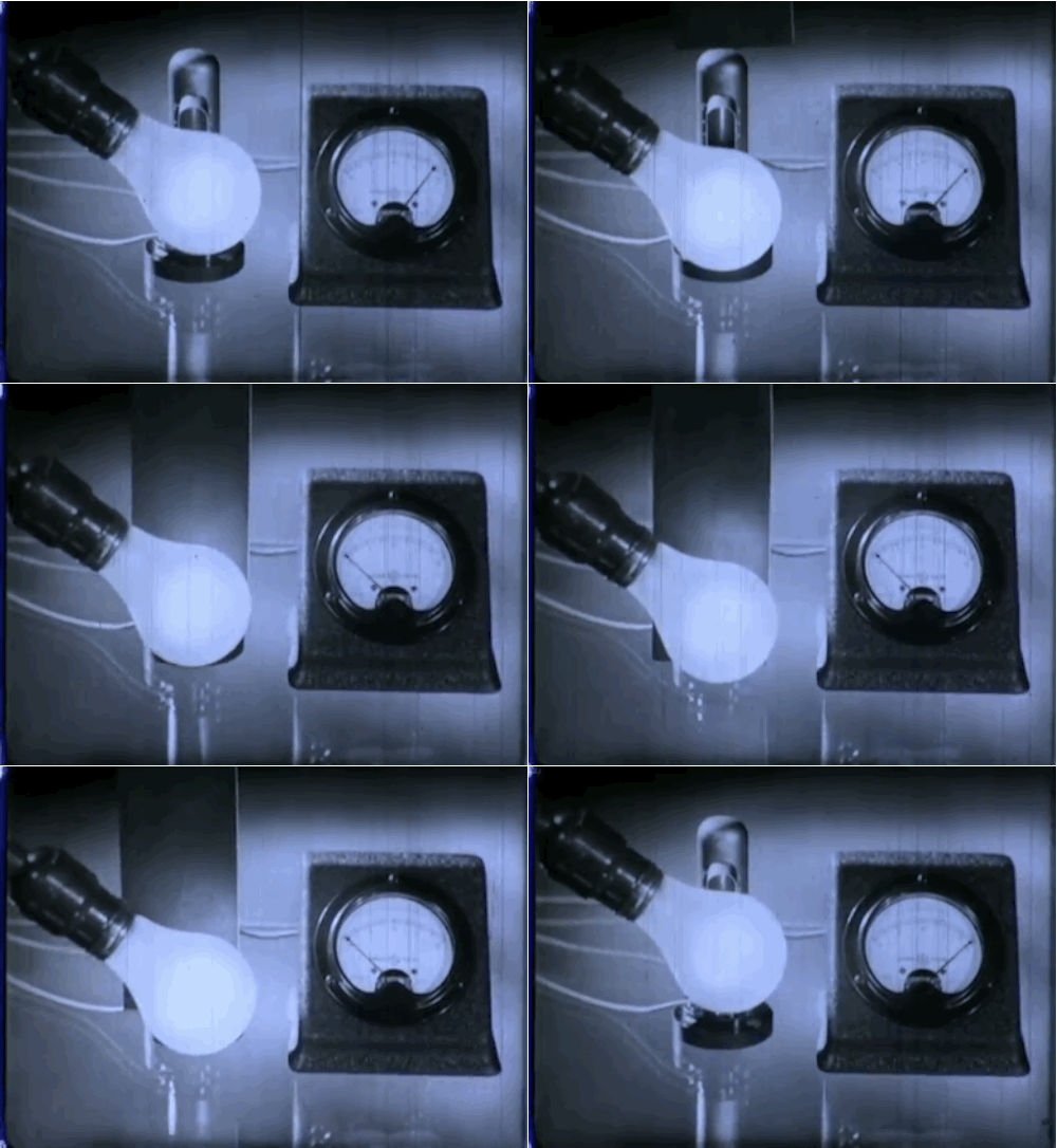
Phototubes, shown here, emit electrons when exposed to light that produce electrical currents. This 1937 episode of GE’s “Excursions in Science” series came out just as manufacturers were beginning to take the device mainstream. The first commercial application was the reproduction of sound for motion picture films.
Post link
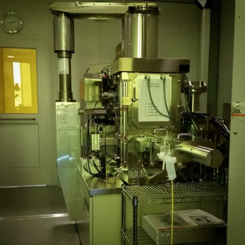
Electron beam lithography is a technique used to write nanometer-size features using a narrow beam of electrons to trace out the desired pattern on your sample. This is a form of maskless lithography - custom patterns can be written without the need for a mask. However, ebeam lithography has a low throughput and it is expensive, making it impractical for industrial purposes. This form of lithography is mainly used in research, mask writing, and prototyping, rather than for mass producing devices.
In the past, I have used this system to make nanowires that are less than 100 nm wide. This is 1/1000th the diameter of a human hair!
Post link
Speed of light looking kinda slow these days… like girl just hurry up

