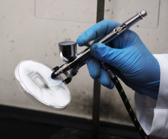
Invigorating the idea of computers based on fluids instead of silicon, researchers at the National Institute of Standards and Technology (NIST) have shown how computational logic operations could be performed in a liquid medium by simulating the trapping of ions (charged atoms) in graphene (a sheet of carbon atoms) floating in saline solution. The scheme might also be used in applications such as water filtration, energy storage or sensor technology.
The idea of using a liquid medium for computing has been around for decades, and various approaches have been proposed. Among its potential advantages, this approach would require very little material and its soft components could conform to custom shapes in, for example, the human body.
NIST’s ion-based transistor and logic operations are simpler in concept than earlier proposals. The new simulations show that a special film immersed in liquid can act like a solid silicon-based semiconductor. For example, the material can act like a transistor, the switch that carries out digital logic operations in a computer. The film can be switched on and off by tuning voltage levels like those induced by salt concentrations in biological systems.
As silicon-based semiconductors reach their performance limits, gallium nitride (GaN) is becoming the next go-to material to advance light-emitting diode (LED) technologies, high-frequency transistors and photovoltaic devices. Holding GaN back, however, is its high numbers of defects.
This material degradation is due to dislocations—when atoms become displaced in the crystal lattice structure. When multiple dislocations simultaneously move from shear force, bonds along the lattice planes stretch and eventually break. As the atoms rearrange themselves to reform their bonds, some planes stay intact while others become permanently deformed, with only half planes in place. If the shear force is great enough, the dislocation will end up along the edge of the material.
Layering GaN on substrates of different materials makes the problem that much worse because the lattice structures typically don’t align. This is why expanding our understanding of how GaN defects form at the atomic level could improve the performance of the devices made using this material.
A team of researchers has taken a significant step toward this goal by examining and determining six core configurations of the GaN lattice. They presented their findings in the Journal of Applied Physics.
UCLA materials scientists and colleagues have discovered that perovskites, a class of promising materials that could be used for low-cost, high-performance solar cells and LEDs, have a previously unutilized molecular component that can further tune the electronic property of perovskites.
Named after Russian mineralogist Lev Perovski, perovskite materials have a crystal-lattice structure of inorganic molecules like that of ceramics, along with organic molecules that are interlaced throughout. Up to now, these organic molecules appeared to only serve a structural function and could not directly contribute to perovskites’ electronic performance.
Led by UCLA, a new study shows that when the organic molecules are designed properly, they not only can maintain the crystal lattice structure, but also contribute to the materials’ electronic properties. This discovery opens up new possibilities to improve the design of materials that will lead to better solar cells and LEDs. The study detailing the research was recently published in Science.
The miniaturization of spectroscopic measurement devices opens novel information channels in medical science and consumer electronics. Scientists of the University of Stuttgart, Germany, developed a 3-D-printed miniature spectrometer with a volume of 100 by 100 by 300 μm3 and a spectral resolution of up to 10 nm in the visible range. This spectrometer can be manufactured directly onto camera sensors, and a parallel arrangement allows for quick (“snapshot”) and low-profile, highly customizable hyperspectral cameras.
Femtosecond direct-laser writing as a 3-D printing technology has been one of the key building blocks for miniaturization in recent years. It has transformed the field of complex micro-optics since the early 2000s. Medical engineering and consumer electronics benefit from these developments. It is now possible to create robust, monolithic and nearly perfectly aligned freeform optical systems on almost arbitrary substrates such as image sensors or optical fibers.
Simultaneously, the miniaturization of spectroscopic measurement devices has been advanced with quantum dot and nanowire technology. These are based on computational approaches, which have the drawback of being calibration-sensitive and require complex reconstruction algorithms.
Scientists Reduce All-Solid-State Battery Resistance by Heating
All-solid-state batteries are now one step closer to becoming the powerhouse of next-generation electronics as researchers from Tokyo Tech, AIST, and Yamagata University introduce a strategy to restore their low electrical resistance. They also explore the underlying reduction mechanism, paving the way for a more fundamental understanding of the workings of all-solid-state lithium batteries.
All-solid-state lithium batteries have become the new craze in materials science and engineering as conventional lithium-ion batteries can no longer meet the standards for advanced technologies, such as electric vehicles, which demand high energy densities, fast charging, and long cycle lives. All-solid-state batteries, which use a solid electrolyte instead of a liquid electrolyte found in traditional batteries, not only meet these standards but are comparatively safer and more convenient as they have the possibility to charge in a short time.
Researchers from the Camborne School of Mines have identified methods to predict the environmental and social cost of resourcing new deposits of rare earth minerals used in the production of mobile phones, wind turbines and electric vehicles.
The team are pioneering techniques to develop the equivalent of a ‘Fairtrade’ model for ethically and sustainably resourcing raw materials that are crucial in the manufacturing of next generation technologies.
In the research the team highlight the pivotal role that geoscientists can play in developing 'life cycle assessment techniques" for potential new deposits of rare earth elements, to meet the growing worldwide demand.
The research is published in the journal, Elements.
Robert Pell, PhD student at the Camborne School of Mines, based at the University of Exeter’s Penryn Campus in Cornwall, and co-author on the paper said, 'It is important that we understand the environmental costs of generating these rare earths so that we can select the right projects to support, but also research and improve the areas of production with a greater environmental cost. This is especially important when you consider the demand growth of rare earths, and their importance in the proliferation of green technology.“
The trick is to be able to use beryllium atoms in gallium nitride. Gallium nitride is a compound widely used in semiconductors in consumer electronics from LED lights to game consoles. To be useful in devices that need to process considerably more energy than in your everyday home entertainment, though, gallium nitride needs to be manipulated in new ways on the atomic level.
[…]
“There is growing demand for semiconducting gallium nitride in the power electronics industry. To make electronic devices that can process the amounts of power required in, say, electric cars, we need structures based on large-area semi-insulating semiconductors with properties that allow minimising power loss and can dissipate heat efficiently. To achieve this, adding beryllium into gallium nitride - or ‘doping’ it - shows great promise,” explains Professor Filip Tuomisto from Aalto University.
Tesla has revealed its Tesla Semi – an articulated lorry that can travel 500 miles (804km) on a single charge, consuming less than two kilowatt-hours of energy per mile.
With a full 80,000-pound load, the lorry can do 0-60 mph in 20 seconds and can climb 5% gradients at 65mph. The electric vehicle’s battery is reinforced for safety and its windshield is made from impact resistant glass.
According to Chief Executive Elon Musk the Tesla Semi could travel 643km after 30 minutes of charging using one of Tesla’s new mega-chargers. While the lorry’s cost has not yet been revealed, Tesla claims that is will be cheaper than diesel equivalents per mile, considering fuel and maintenance.
The Tesla Semi is due to go into production in 2019.
To find out more on materials science, packaging and engineering news, visit our website IOM3 at or follow us on Twitter @MaterialsWorld for regular news updates.
The remarkable properties of 2-D materials—made up of a single layer of atoms—have made them among the most intensely studied materials of our time. They have the potential to usher in a new generation of improved electronics, batteries and sensory devices, among other applications.
One obstacle to realizing applications of these materials is the cost and time needed for experimental studies. However, computer simulations are helping researchers overcome this challenge in order to accurately characterize material structures and functions at an accelerated pace.
At the U.S. Department of Energy’s (DOE) Argonne National Laboratory, researchers have simulated the growth of silicene, a 2-D material with attractive electronic properties. Their work, published in Nanoscale, delivers new and useful insights on the material’s properties and behavior and offers a predictive model for other researchers studying 2-D materials.
Going forward, this model can accelerate researchers’ understanding of 2-D materials, and bring us closer to realizing their applications within a wide range of industries.
A research team led by Dr. Byeong-dae Choi of DGIST’s Intelligent Devices and Systems Research Group has developed an electroluminescent film that is four times brighter than existing ones. The new film can improve the luminance of electroluminescent devices by 422 percent compared to conventional ones by applying retro-reflection electrodes that adapt the principle of nocturnal animal eyes.
Electroluminescent (EL) refers to an optical and electrical phenomenon in which a material emits light in response to the passage of an electric current. Electroluminescent films using phosphor powder have advantages such as excellent durability in a deformed state due to flexibility and elasticity, and high efficiency despite low cost. However, it was difficult to put into practical use due to their low brightness.
In order to increase the brightness of electroluminescent devices, the research team paid attention to the eyes of nocturnal animals with high utilization efficiency of light. The researchers used the retro-reflection characteristics that the light returns to the light source without being dispersed in the retroreflective structure of the nocturnal animal eye while it is scattered in the normal reflection structure.
Current silicon-based computing technology is energy-inefficient. Information and communications technology is projected to use over 20% of global electricity production by 2030. So finding ways to decarbonise technology is an obvious target for energy savings. Professor Paolo Radaelli from Oxford’s Department of Physics, working with Diamond Light Source, the U.K.“s national synchrotron, has been leading research into more efficient alternatives to silicon. His group’s surprising findings are published in Nature in an article titled "Antiferromagnetic half-skyrmions and bimerons at room temperature.” Some of the antiferromagnetic textures they have found could emerge as prime candidates for low-energy antiferromagnetic spintronics at room temperature.
Researchers have been working for a long time on alternative technologies to silicon. Oxides of common metals such as iron and copper are natural targets because they are already a technology staple, present in silicon-based computers, meaning there is a high chance of compatibility between the two technologies. Although oxides are great for storing information, they are not good at moving information around—a necessity for computation. However, one property of oxides that has emerged is that many are magnetic, which means it might be possible to move magnetic bits around, both in oxides and in other magnets, with very little energy required.
Piezoelectric materials hold great promise as sensors and as energy harvesters but are normally much less effective at high temperatures, limiting their use in environments such as engines or space exploration. However, a new piezoelectric device developed by a team of researchers from Penn State and QorTek remains highly effective at elevated temperatures.
Clive Randall, director of Penn State’s Materials Research Institute (MRI), developed the material and device in partnership with researchers from QorTek, a State College, Pennsylvania-based company specializing in smart material devices and high-density power electronics.
“NASA’s need was how to power electronics in remote locations where batteries are difficult to access for changing,” Randall said. “They also wanted self-powering sensors that monitor systems such as engine stabilities and have these devices work during rocket launches and other high-temperature situations where current piezoelectrics fail due to the heat.”
by Yury Gogotsi, Asia Sarycheva, and Babak Anasori
Spraying an antenna onto a flat surface. Drexel University Nanomaterials Lab, CC BY-ND
Hear the word “antenna” and you might think about rabbit ears on the top of an old TV or the wire that picks up radio signals for a car. But an antenna can be much smaller – even invisible. No matter its shape or size, an antenna is crucial for communication, transmitting and receiving radio signals between devices. As portable electronics become increasingly common, antennas must, too.
Wearable monitors, flexible smart clothes, industrial sensors and medical sensors will be much more effective if their antennas are lightweight and flexible – and possibly even transparent. We and our collaborators have developed a type of material that offers many more options for connecting antennas to devices – including spray-painting them on walls or clothes.
A new type of battery developed by researchers at MIT could be made partly from carbon dioxide captured from power plants. Rather than attempting to convert carbon dioxide to specialized chemicals using metal catalysts, which is currently highly challenging, this battery could continuously convert carbon dioxide into a solid mineral carbonate as it discharges.
The battery is made from lithium metal, carbon, and an electrolyte that the researchers designed. While still based on early-stage research and far from commercial deployment, the new battery formulation could open up new avenues for tailoring electrochemical carbon dioxide conversion reactions, which may ultimately help reduce the emission of the greenhouse gas to the atmosphere.
Currently, power plants equipped with carbon capture systems generally use up to 30 percent of the electricity they generate just to power the capture, release, and storage of carbon dioxide. Anything that can reduce the cost of that capture process, or that can result in an end product that has value, could significantly change the economics of such systems, the researchers say.
Betar Gallant, Assistant Professor of Mechanical Engineering at MIT, said, ‘Carbon dioxide is not very reactive. Trying to find new reaction pathways is important.’Ideally, the gas would undergo reactions that produce something worthwhile, such as a useful chemical or a fuel. However, efforts at electrochemical conversion, usually conducted in water, remain hindered by high energy inputs and poor selectivity of the chemicals produced.
The team looked into whether carbon-dioxide-capture chemistry could be put to use to make carbon-dioxide-loaded electrolytes — one of the three essential parts of a battery — where the captured gas could then be used during the discharge of the battery to provide a power output.
The team developed a new approach that could potentially be used right in the power plant waste stream to make material for one of the main components of a battery. By incorporating the gas in a liquid state, however, Gallant and her co-workers found a way to achieve electrochemical carbon dioxide conversion using only a carbon electrode. The key is to preactivate the carbon dioxide by incorporating it into an amine solution.
‘What we’ve shown for the first time is that this technique activates the carbon dioxide for more facile electrochemistry,’ Gallant says. ‘These two chemistries — aqueous amines and nonaqueous battery electrolytes — are not normally used together, but we found that their combination imparts new and interesting behaviors that can increase the discharge voltage and allow for sustained conversion of carbon dioxide.’
The battery is made from lithium metal, carbon, and an electrolyte that the researchers designed. While still based on early-stage research and far from commercial deployment, the new battery formulation could open up new avenues for tailoring electrochemical carbon dioxide conversion reactions, which may ultimately help reduce the emission of the greenhouse gas to the atmosphere.
Printed electronics use standard printing techniques to manufacture electronic devices on different substrates like glass, plastic films, and paper. Interest in this area is growing because of the potential to create cheaper circuits more efficiently than conventional methods. A new study by researchers at Soonchunhyang University in South Korea, published in AIP Advances, provides insights into the processing of copper nanoparticle ink with green laser light.
Kye-Si Kwon and his colleagues previously worked with silver nanoparticle ink, but they turned to copper (derived from copper oxide) as a possible low-cost alternative. Metallic inks composed of nanoparticles hold an advantage over bulk metals because of their lower melting points. Although the melting point of copper is about 1,083 degrees Celsius in bulk, according to Kwon, copper nanoparticles can be brought to their melting point at just 150 to 500 C—through a process called sintering. Then, they can be merged and bound together.
Kwon’s group concentrates on photonic approaches for heating nanoparticles by the absorption of light. “A laser beam can be focused on a very small area, down to the micrometer level,” explained Kwon and doctorate student Md. Khalilur Rahman. Heat from the laser serves two main purposes: converting copper oxide into copper and promoting the conjoining of copper particles through melting.
Computers may be growing smaller and more powerful, but they require a great deal of energy to operate. The total amount of energy the U.S. dedicates to computing has risen dramatically over the last decade and is quickly approaching that of other major sectors, like transportation.
In a study published online this week the journal Nature, University of California, Berkeley, engineers describe a major breakthrough in the design of a component of transistors—the tiny electrical switches that form the building blocks of computers—that could significantly reduce their energy consumption without sacrificing speed, size or performance. The component, called the gate oxide, plays a key role in switching the transistor on and off.
“We have been able to show that our gate-oxide technology is better than commercially available transistors: What the trillion-dollar semiconductor industry can do today—we can essentially beat them,” said study senior author Sayeef Salahuddin, the TSMC Distinguished professor of Electrical Engineering and Computer Sciences at UC Berkeley.
The direct band gap of AlN-based materials makes them suitable for fabricating DUV optoelectronic devices, which have a wide range of application prospects in the fields of curing, water and air disinfection, medicine and biochemistry. Therefore, achieving a high-quality epitaxy of AlN films is of particular importance to ensure the excellent performance of DUV photoelectric devices.
Currently, due to the lack of cost-effective homogenous substrates, the optimal choice to grow AlN films is usually to perform heteroepitaxial growth on sapphire. Unfortunately, the inherent mismatches between AlN and sapphire substrate inevitably introduce a variety of crystalline defects into the AlN epilayer. In particular, the large residual strain in the AlN film leads to the nonuniformity of the Al distribution in the upper AlGaN layer accompanied by wafer bending, which severely limits the device performance. Therefore, a feasible strategy is required to make a qualitative leap to realize high-quality growth of heteroepitaxial AlN films and to meet the application requirements of DUV optoelectronic devices.
Researchers have created a stretchy transistor that can be elongated to twice its length with only minimal changes in its conductivity. The development is a valuable advancement for the field of wearable electronics. To date, it has been difficult to design a transistor using inherently stretchable materials that maintains its conductivity upon being stretched.
Here, Jie Xu and devise a clever and scalable way to confine organic conductors inside a rubbery polymer to create stretchy transistors. They took a semiconducting polymer, called DPPT-TT, and confined it inside another polymer, SEBS, which has elastic properties.
As the two polymers don’t like to mix with each other, the DPPT-TT forms thin bundles within the SEBS matrix. Testing and analysis of this new combination reveal that it works as an effective transistor, even as it is repeatedly stretched up to 100% of its length. While the material demonstrated a normal conductivity of 0.59 cm2/Vs on average, this dropped only slightly to 0.55 cm2/Vs when being stretched to twice its length.
Scientists at the U.S. Naval Research Laboratory (NRL), Materials Science and Technology Division, have demonstrated that the intensity and spectral composition of the photoluminescence emitted from a single monolayer of tungsten disulphide (WS2) can be spatially controlled by the polarization domains in an adjacent film of the ferroelectric material lead zirconium titanate (PZT).
These domains are written in the PZT using a conductive atomic force microscope, and the photoluminescence (PL) is measured in air at room temperature. Because the polarization domain wall width in a ferroelectric can be as low as 1-10 nm, this approach enables spatial modulation of PL intensity and the corresponding carrier populations with potential for nanoscale resolution.
Single monolayer transition metal dichalcogenides (TMDs) such as WS2 exhibit striking optical properties due to their direct band gap. The dielectric screening is very low due to their two dimensional (2D) character, and thus their properties are strongly affected by their immediate environment, and can be modified and controlled by variations in local charge density due to adsorbates or electrostatic gating. This has generated keen interest in a wide variety of electronic and optical device applications.
You can now 3D print lithium-ion batteries in any shape.
Lithium-ion batteries are normally either cylindrical or rectangular shaped, which forces manufacturers to dedicate a certain size and place for the battery in its design. This way of making electronic devices such as laptops and mobile phones may cause a waste of both space and options to branch out with design.
InACS Applied Energy Materials, researchers present their method of 3D printing which can create the whole structural device, including the battery and with all the electronic components – in almost any shape.
Since the polymers used for printing, like poly(lactic acid) (PLA) are not ionic conductors, the researchers infused PLA with an electrolyte solution as well as adding graphene into the anode or cathode to boost the battery’s electrical conductivity.
Showing the capacity of the printed battery, the team printed a bracelet with an integrated battery. As of now, the battery could only power the green LED for approximately 60 seconds – making the battery circa two orders of magnitude lower than already commercially available batteries. Although this makes the battery capacity too low to use at the moment, the researchers have multiple ideas to fix the low capacity such as, replacing the PLA materials with 3D printable pastes.