#transistors
Simple logic for nanofluidic computing simulated
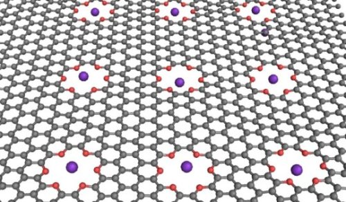
Invigorating the idea of computers based on fluids instead of silicon, researchers at the National Institute of Standards and Technology (NIST) have shown how computational logic operations could be performed in a liquid medium by simulating the trapping of ions (charged atoms) in graphene (a sheet of carbon atoms) floating in saline solution. The scheme might also be used in applications such as water filtration, energy storage or sensor technology.
The idea of using a liquid medium for computing has been around for decades, and various approaches have been proposed. Among its potential advantages, this approach would require very little material and its soft components could conform to custom shapes in, for example, the human body.
NIST’s ion-based transistor and logic operations are simpler in concept than earlier proposals. The new simulations show that a special film immersed in liquid can act like a solid silicon-based semiconductor. For example, the material can act like a transistor, the switch that carries out digital logic operations in a computer. The film can be switched on and off by tuning voltage levels like those induced by salt concentrations in biological systems.
Post link
Engineered crystals could help computers run on less power
Computers may be growing smaller and more powerful, but they require a great deal of energy to operate. The total amount of energy the U.S. dedicates to computing has risen dramatically over the last decade and is quickly approaching that of other major sectors, like transportation.
In a study published online this week the journal Nature, University of California, Berkeley, engineers describe a major breakthrough in the design of a component of transistors—the tiny electrical switches that form the building blocks of computers—that could significantly reduce their energy consumption without sacrificing speed, size or performance. The component, called the gate oxide, plays a key role in switching the transistor on and off.
“We have been able to show that our gate-oxide technology is better than commercially available transistors: What the trillion-dollar semiconductor industry can do today—we can essentially beat them,” said study senior author Sayeef Salahuddin, the TSMC Distinguished professor of Electrical Engineering and Computer Sciences at UC Berkeley.
Post link
A flexible transistor that conforms to skin
Researchers have created a stretchy transistor that can be elongated to twice its length with only minimal changes in its conductivity. The development is a valuable advancement for the field of wearable electronics. To date, it has been difficult to design a transistor using inherently stretchable materials that maintains its conductivity upon being stretched.
Here, Jie Xu and devise a clever and scalable way to confine organic conductors inside a rubbery polymer to create stretchy transistors. They took a semiconducting polymer, called DPPT-TT, and confined it inside another polymer, SEBS, which has elastic properties.
As the two polymers don’t like to mix with each other, the DPPT-TT forms thin bundles within the SEBS matrix. Testing and analysis of this new combination reveal that it works as an effective transistor, even as it is repeatedly stretched up to 100% of its length. While the material demonstrated a normal conductivity of 0.59 cm2/Vs on average, this dropped only slightly to 0.55 cm2/Vs when being stretched to twice its length.
Post link
Scientists move graphene closer to transistor applications
Scientists at the U.S. Department of Energy’s Ames Laboratory were able to successfully manipulate the electronic structure of graphene, which may enable the fabrication of graphene transistors— faster and more reliable than existing silicon-based transistors.
The researchers were able to theoretically calculate the mechanism by which graphene’s electronic band structure could be modified with metal atoms. The work will guide experimentally the use of the effect in layers of graphene with rare-earth metal ions “sandwiched” (or intercalated) between graphene and its silicon carbide substrate. Because the metal atoms are magnetic the additions can also modify the use of graphene for spintronics.
“We are discovering new and more useful versions of graphene,” said Ames Laboratory senior scientist Michael C. Tringides. “We found that the placement of the rare earth metals below graphene, and precisely where they are located, in the layers between graphene and its substrate, is critical to manipulating the bands and tune the band gap.”
Post link
An exotic material called gallium nitride (GaN) is poised to become the next semiconductor for power electronics, enabling much higher efficiency than silicon. In 2013, the Department of Energy (DOE) dedicated approximately half of a $140 million research institute for power electronics to GaN…
Making the internet of things possible with a new breed of ‘memristors’
Easily printable, organic thin films can retain data for more than 10 years without power, work with low voltages – and become the building block of future computers that mimic the human brain
The internet of things is coming, that much we know. But still it won’t; not until we have components and chips that can handle the explosion of data that comes with IoT. In 2020, there will already be 50 billion industrial internet sensors in place all around us. A single autonomous device – a smart watch, a cleaning robot, or a driverless car – can produce gigabytes of data each day, whereas an airbus may have over 10,000 sensors in one wing alone.
Two hurdles need to be overcome. First, current transistors in computer chips must be miniaturized to the size of only few nanometres; the problem is they won’t work anymore then. Second, analysing and storing unprecedented amounts of data will require equally huge amounts of energy. Sayani Majumdar, Academy Fellow at Aalto University, along with her colleagues, is designing technology to tackle both issues.
Majumdar has with her colleagues designed and fabricated the basic building blocks of future components in what are called “neuromorphic” computers inspired by the human brain. It’s a field of research on which the largest ICT companies in the world and also the EU are investing heavily. Still, no one has yet come up with a nano-scale hardware architecture that could be scaled to industrial manufacture and use.
Post link
See-through circuitry: New method makes AZO a viable and cheap alternative for transparent electronics
Indium tin oxide (ITO) is the current material of choice for electronics because it combines optical transparency with electrical conductivity. Its use ranges from touch-sensitive smartphone screens to light-harvesting solar panels. Indium is in short supply, however, and as demand increases for ITO-containing devices, so does the price of indium.
One promising low-cost ITO alternative is a transparent material known as aluminum-doped zinc oxide (AZO).
“The elements that make up this material are more abundant than indium, making AZO a commercially sensible option,” said Professor Husam Alshareef from the KAUST Physical Science and Engineering Division who also led the research. “However, electronic devices made using AZO have traditionally shown inferior performance to devices made using ITO.”
Post link
Electronic circuits printed at one micron resolution
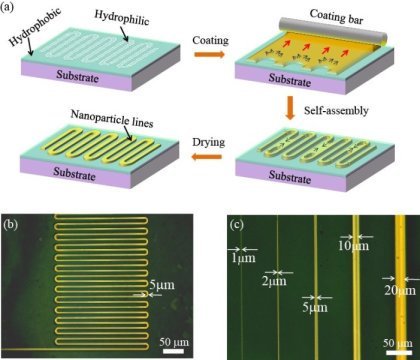
A research team consisting of MANA Independent Scientist Takeo Minari, International Center for Materials Nanoarchitectonics (MANA), NIMS, and Colloidal Ink developed a printing technique for forming electronic circuits and thin-film transistors (TFTs) with line width and line spacing both being 1 μm. Using this technique, the research team formed fully-printed organic TFTs with a channel length of 1 μm on flexible substrates, and confirmed that the TFTs operate at a practical level.
Printed electronics – printing techniques to fabricate electronic devices using functional materials dissolved in ink – is drawing much attention in recent years as a promising new method to create large-area semiconductor devices at low cost. Because these techniques enable the formation of electronic devices even on flexible substrates, they are expected to be applicable to new fields such as wearable devices. In comparison, conventional printing technologies allow the formation of circuits and devices with line widths only as narrow as several dozen micrometers. Accordingly, they are not applicable to the creation of minute devices suitable for practical use. Thus, there were high expectations for developing new printing techniques capable of consistently fabricating circuits with line widths of several micrometers or less.
Post link
October 18, 1954: Texas Instruments unveils the transistor radio. When asked how they could build a radio so small, the groundbreaking tech company credits “ear spirits.”


