#optoelectronics
Closing the gap: On the road to terahertz electronics
Asymmetric plasmonic antennas deliver femtosecond pulses for fast optoelectronics
A team headed by the TUM physicists Alexander Holleitner and Reinhard Kienberger has succeeded for the first time in generating ultrashort electric pulses on a chip using metal antennas only a few nanometers in size, then running the signals a few millimeters above the surface and reading them in again a controlled manner.
Classical electronics allows frequencies up to around 100 gigahertz. Optoelectronics uses electromagnetic phenomena starting at 10 terahertz. This range in between is referred to as the terahertz gap, since components for signal generation, conversion and detection have been extremely difficult to implement.
The TUM physicists Alexander Holleitner and Reinhard Kienberger succeeded in generating electric pulses in the frequency range up to 10 terahertz using tiny, so-called plasmonic antennas and run them over a chip. Researchers call antennas plasmonic if, because of their shape, they amplify the light intensity at the metal surfaces.
Post link
Research on light-matter interaction could improve electronic and optoelectronic devices
Fundamental research sheds light on new many-particle quantum physics in atomically thin semiconductors
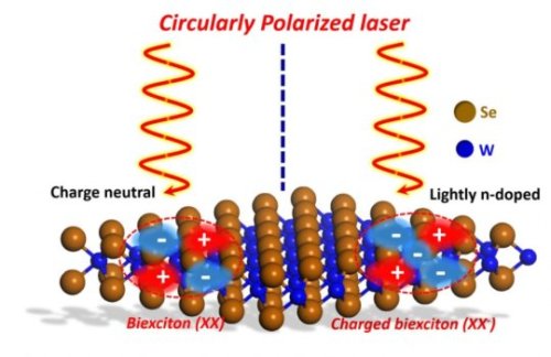
A paper published in Nature Communications by Sufei Shi, assistant professor of chemical and biological engineering at Rensselaer, increases our understanding of how light interacts with atomically thin semiconductors and creates unique excitonic complex particles, multiple electrons, and holes strongly bound together. These particles possess a new quantum degree of freedom, called “valley spin.” The “valley spin” is similar to the spin of electrons, which has been extensively used in information storage such as hard drives and is also a promising candidate for quantum computing.
The paper, titled “Revealing the biexciton and trion-exciton complexes in BN encapsulated WSe2,” was published in the Sept. 13, 2018, edition of Nature Communications. Results of this research could lead to novel applications in electronic and optoelectronic devices, such as solar energy harvesting, new types of lasers, and quantum sensing.
Shi’s research focuses on low dimensional quantum materials and their quantum effects, with a particular interest in materials with strong light-matter interactions. These materials include graphene, transitional metal dichacogenides (TMDs), such as tungsten diselenide (WSe2), and topological insulators.
Post link
Digitally programmable perovskite nanowire-block copolymer composites
One-dimensional nanomaterials with highly anisotropicoptoelectronic properties can be used within energy harvesting applications, flexible electronics and biomedical imaging devices. In materials science and nanotechnology, 3-D patterning methods can be used to precisely assemble nanowires with locally controlled composition and orientation to allow new optoelectronic device designs. In a recent report, Nanjia Zhou and an interdisciplinary research team at the Harvard University, Wyss Institute of Biologically Inspired Engineering, Lawrence Berkeley National Laboratory and the Kavli Energy Nanoscience Institute developed and 3-D printed nanocomposite inks composed of brightly emitting colloidal cesium lead halide perovskite (CsPbX3, where X= Cl, Br, or I) nanowires.
They suspended the bright nanowires in a polystyrene-polyisoprene-polystyrene block copolymer matrix and defined the nanowire alignment using a programmed print path. The scientist produced optical nanocomposites that exhibited highly polarized absorption and emission properties. To highlight the versatility of the technique they produced several devices, including optical storage, encryption, sensing and full color displays. The work is now published on Science Advances.
Post link
‘Zipping-up’ rings to make nanographenes
A fast and efficient method for graphene nanoribbon synthesis
Nanographenes are attracting wide interest from many researchers as a powerful candidate for the next generation of carbon materials due to their unique electric properties. Scientists at Nagoya University have now developed a fast way to form nanographenes in a controlled fashion. This simple and powerful method for nanographene synthesis could help generate a range of novel optoelectronic materials, such as organic electroluminescent displays and solar cells.
Nagoya, Japan – A group of chemists of the JST-ERATO Itami Molecular Nanocarbon Project and the Institute of Transformative Bio-Molecules (ITbM) of Nagoya University, and their colleagues have developed a simple and powerful method to synthesize nanographenes. This new approach, recently described in the journal Science, is expected to lead to significant progress in organic synthesis, materials science and catalytic chemistry.
Nanographenes, one-dimensional nanometer-wide strips of graphene, are molecules composed of benzene units. Nanographenes are attracting interest as a powerful candidate for next generation materials, including optoelectronic materials, due to their unique electric characteristics. These properties of nanographenes depend mainly on their width, length and edge structures. Thus, efficient methods to access structurally controlled nanographenes is highly desirable.
Post link


