At extremely small scales, looks can be deceiving. While at first glance you might see lily pads floating on a tranquil pond, this image is actually a clever adaptation of a snapshot taken on a scanning electron microscope.
In reality, the green spots are only a few micrometers across—smaller than width of a human hair. They make up a surface coating that was developed to limit the transmission of SARS-CoV-2, the virus that causes COVID-19. The coating is composed of a silver-based material applied to a glass surface. The lotus flower, though, was some added artistic flair courtesy of image-editing software.
Mohsen Hosseini, Ph.D. candidate in chemical engineering, and William Ducker, professor of chemical engineering, recently won an award in the National Nanotechnology Coordinated Infrastructure (NNCI) image contest with this image. Both Hosseini and Ducker are affiliated with the Macromolecules Innovation Institute (MII).
Reverse osmosis is used worldwide to purify drinking water. It is deployed at extremely large scales in desalination plants and is a leading technology in potable water reuse, also called toilet-to-tap—a nickname that annoys scientists and engineers working on potable water reuse. Though existing reverse osmosis membranes remove salt and most contaminants, a few slip through, such as boron and N-nitrosodimethylamine (NDMA), a toxic byproduct of the chlorination used upstream to kill pathogens. To make a better membrane, a team from China’s State Key Laboratory of Pollution Control and Resource Reuse, the University of Hong Kong, and Vanderbilt University used nanoflakes of an amphiphilic metal-organic framework (MOF) to create a next-generation polyamide membrane. The MOF flakes line up on the interface between the water and hexane emulsion where amide polymerization takes places, regulating the heat and mass transfer associated with the reaction. In this microscope image, the researchers whipped the mixture into an emulsion to probe how the MOFs behave at the interface. The final result is a thin, crumpled membrane material that outperforms conventional membranes in removing salt, boron, and NDMA. —Craig Bettenhausen
These colors are real! Looking at a section under polarizing light can be used to identify minerals through their index of refraction by matching the vivid colors seen here to a handy-dandy chart. Rotating the specimen can reveal diagnostic features like tartan twinning on the left (microcline) or undulose extinction (quartz).
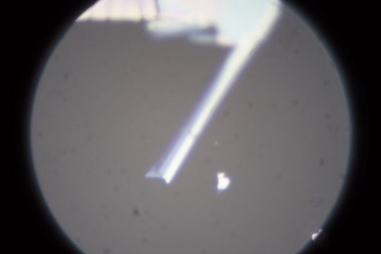
I finally got to try my hand at sample preparation these past 2 weeks. Materials can exhibit striking electronic and mechanical properties when stripped to few layers / monolayer. Graphene (single layer graphite) is one popular example, first to be discovered among the family of 2D materials in 2004. But the search for conducting 2D materials has now extended beyond graphene.
I tried to exfoliate a single layer of molybdenum disulfide (MoS2), one type of transition metal dichalcogenides (TMD), under the guidance of my lab colleague. The properties of these TMD in the form of 2D sheets have application in more efficient electronics, semiconductors, solar cells, and touch screen display panels, just to name a few.
Exfoliation in this context is actually applying the material of interest onto a scotch tape, then folding and opening the tape several times until the flakes on it are as thin as possible. Judging with my naked eyes, this usually just means for the flakes to not appear as shiny (for metal compounds) anymore. Then, I will have to transfer the flakes on the Scotch tape to a tiny piece of transparent gel (PDMS gel). The procedure is pretty simple, but the flakes produced are not guaranteed to be thin enough. Through my many trials, I find random thickness of flakes distributed all over the gel under optical microscope. And among them, we need to locate the thinnest of all that could potentially be a monolayer.
Below is the flake that I suspect to be a single layer of MoS2 at different magnification level. Can you find it in the last picture?
Here is the relative size of the PDMS gel on which all these flakes lie.
This also happened when I managed to transfer plenty of flakes onto the PDMS gel, while most of the time I do not get enough to choose from when observed under the microscope. After identifying this flake, I had to transfer it onto another substrate (such as a silicon nitride grid), before I can put it into an electron microscope that offer higher resolution through electrons scattering method. The transfer patience takes some patience, as pressing or lifting the gel too quickly may break the hard-found flake. So it is just a lot of going back and forth between the sample preparation table and microscope to get one nice specimen. But it is important to get through this process for us to get to the characterization part, which is where all the fun stuff about science comes in!
Further information: The micrograph shows primary Al dendrite arms (white). The dendrite trunk has been intersected at an angle by the plane of polishing to give the observed morphology. Between the dendrites is the Al - CuAl2 eutectic. Initially dendrites would have formed from the liquid, the regions between the dendrite arms known as the mushy zone transforming to a eutectic solid (L to Al + CuAl2). These two phases form cooperatively as neighbouring lamellae with the lateral diffusion of material across the growing interface. The relative amounts of the two phases (Al and CuAl2 ) within the eutectic are determined by applying the Lever Rule at the eutectic temperature.
NanorosesBy Vilas G. Pol These tiny crystalline “roses” of europium oxycarbonate are formed under intense heat and pressure in a controlled system. Under certain conditions, they emit bright red light. Scientists are working to investigate the material’s luminescence intensity and decay time. Europium oxide, a related compound, has proven useful in lasers and high-density optical storage devices, and researchers hope to discover more about this unusual oxycarbonate compound and its potential applications. Previously published: Pol V.G. et al. Inorg. Chem. 2009, 48, 5569–5573
At microscopic scales, even a clean break isn’t very clean - this electron microscope picture is of the edge of a piece of glass, on which I had fabricated a long wall of semiconductor (the long columned wall you see at the middle right). I had zoomed in on this spot to make sure the wall went all the way to the edge of the glass. What I didn’t expect to see were these little guys clustered near the edge, seeming to look out over into the abyss. They were probably formed by little bits of debris (their little hats), that flew from the edge when it was cut. Since I made the nearby wall by etching away all of the semiconductor that wasn’t protected by a glassy wall-shaped mask, the same etching process left behind all the areas that were protected by the little debris hats. They’re small - if you stacked 200 of them on top of each other, they’d just about equal the thickness of a single human hair.
So this is a Scanning Electron Microscope (SEM) photo I took today of one of my samples of tungsten (VI) oxide, this is the sample marketed as <20 micrometers (10^-6 m ) in diameter. As you can see there are some particles that at bigger than this which tells you that suppliers can’t be trusted with what they say…
But It also shows that the particles are not regular shapes which can effect the stability of the emulsions formed with them. This was what the powder looks like as it has been supplied, if I was to sonicate this the particles should be much smaller on average
I just thought it was a really nice picture and there you go
Unexpected Beauty by FEI Company Via Flickr: It’s a contamination of iron oxide involving the tungsten filament of an automotive light bulb. Courtesy of Mr. FRANCISCO RANGEL , MCT/INT Image Details Instrument used: Quanta SEM Magnification:3963xHorizontal Field Width: 75.3 μm Vacuum: 9.27e-7 mbar Voltage: 20 kV Spot:2.0Working Distance:10.8Detector: Mix: SE plus BSE.
Chopped woodpile by FEI Company Via Flickr: Rough cut into structured IP photoresist. Structure was written with the 3D laser lithography system Nanoscribe. The „woodpile“ was milled for an inside analysis. Courtesy of Dr. Thomas Loeber , TU Kaiserslautern NSC Image Details Instrument used: Helios NanoLab Magnification:3,500Horizontal Field Width:59,2Voltage: 2 kV Working Distance:3,7Detector:SE
Researchers want to develop biocompatible polymers that would serve as scaffolding that helps regrow tissue, replacing damaged or missing flesh and organs in patients. A Swedish team developed the high-molecular-weight polymer shown above, which fluoresces strongly under near-infrared light, a part of the spectrum where most flesh is transparent. In lab rats, the researchers monitored the scaffolding mats with near-IR light and observed that it was colonized by rat tissue and blood vessels.
False-colour electron microscope image of the silicon nanoelectronic device which contains the phosphorus atom used for the demonstration of quantum entanglement. Credit: University of New South Wales
This image may look torn from the pages of a horror novel, but it actually depicts a possible new manufacturing method for electronic devices that work with living tissues. A team at Georgia Tech is studying the use of protein biofilms to direct the orderly formation of semiconducting polymer chains. Greater order in the chains could mean better and more predictable electronic properties for devices such as biocompatible sensors or electrodes. The researchers mixed poly(3-hexylthiophene) with a fungal protein called cerato-ulmin in the solvent 1,2,4-trichlorobenzene. As the proteins assembled into biofilms, the polymer collected in stable microstructures (dark areas above). These structures over time formed spindly branches, which slowly budded to release polymer-containing capsules. The team is now working on understanding and controlling the details of this process.
Forging blank (Titanium, grade 1): taken pictures with polarized light || on the left side: oxygenated edge area (needles visible) || on the right side: regular microstructure in the core area
A team led by DESY scientists has designed, fabricated and successfully tested a novel X-ray lens that produces sharper and brighter images of the nano world. The lens employs an innovative concept to redirect X-rays over a wide range of angles, making a high convergence power. The larger the convergence the smaller the details a microscope can resolve, but as is well known it is difficult to bend X-rays by large enough angles. By fabricating a nano-structure that acts like an artificial crystal it was possible to mimic a high refracting power. Although the fabrication needed to be controlled at the atomic level — which is comparable to the wavelength of X-rays — the DESY scientists achieved this precision over an unprecedented area, making for a large working-distance lens and bright images. Together with the improved resolution these are key ingredients to make a super X-ray microscope. The team led by Dr. Saša Bajt from DESY presents the novel lens in the journal Scientific Reports (Nature Publishing Group).
“X-rays are used to study the nano world, as they are able to show much finer details than visible light and their penetrating power allows you to see inside objects,” explains Bajt. The size of the smallest details that can be resolved depends on the wavelength of the radiation used. X-rays have very short wavelengths of only about 1 to 0.01 nanometres (nm), compared to 400 to 800 nm for visible light. A nanometre is a millionth of a millimetre. The high penetration of X-rays is favoured for three-dimensional tomographic imaging of objects such as biological cells, computer chips, and the nanomaterials involved in energy conversion or storage. But this also means that the X-rays pass straight through conventional lenses without being bent or focussed. One possible method to focus X-rays is to merely graze them from the surface of a mirror to nudge them towards a new direction. But such X-ray mirrors are limited in their convergence power and must be mechanically polished to high precision, making them extremely expensive.
Intergranular fractures (shown through SEM images in the four pictures above) are when materials fail along the grain boundaries, often due to imperfections or inclusions at the grain boundaries or hostile environmental or usage conditions.


![Al 75, Cu 25 (wt%), hypoeutectic alloy Processing: Sand cast[…]Sample preparation: Etched in](https://64.media.tumblr.com/79ecb73957bcb39176b5d6c751534161/tumblr_ovkv9cYTp91u00si6o1_500.jpg "Al 75, Cu 25 (wt%), hypoeutectic alloy Processing: Sand cast[…]Sample preparation: Etched in")


 photo I took today of one of my samples")


")


: taken pictures with polarized light || on the left sid")
: taken pictures with polarized light || on the left sid")
: taken pictures with polarized light || on the left sid")
: taken pictures with polarized light || on the left sid")


 are when materials fai")
 are when materials fai")
 are when materials fai")
 are when materials fai")