Kirigami is the Japanese art of paper cutting. Likely derived from the Chinese art of jiǎnzhǐ, it emerged around the 7th century in Japan, where it was used to decorate temples. Still in practice today, the kirigami artist uses one piece of paper to cut decorative designs, like birds and fish or the more intricate and popular snowflake.
But, this ancient art, which relies on exacting cuts to determine or replicate patterns, is finding more modern and practical applications in electronics. Specifically, in the manufacture of 2D stretchable materials that can play host to wearable electronics, like electronic skins for health monitoring.
The process combines the art of kirigami with an artificial intelligence technique called autonomous reinforcement learning. And to better synchronize the old with the new, researchers from the University of Southern California use the computing power available to them at the U.S. Department of Energy’s (DOE) Argonne National Laboratory.
I finally got to try my hand at sample preparation these past 2 weeks. Materials can exhibit striking electronic and mechanical properties when stripped to few layers / monolayer. Graphene (single layer graphite) is one popular example, first to be discovered among the family of 2D materials in 2004. But the search for conducting 2D materials has now extended beyond graphene.
I tried to exfoliate a single layer of molybdenum disulfide (MoS2), one type of transition metal dichalcogenides (TMD), under the guidance of my lab colleague. The properties of these TMD in the form of 2D sheets have application in more efficient electronics, semiconductors, solar cells, and touch screen display panels, just to name a few.
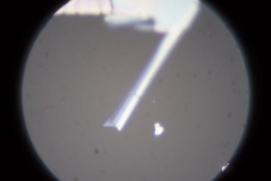
Exfoliation in this context is actually applying the material of interest onto a scotch tape, then folding and opening the tape several times until the flakes on it are as thin as possible. Judging with my naked eyes, this usually just means for the flakes to not appear as shiny (for metal compounds) anymore. Then, I will have to transfer the flakes on the Scotch tape to a tiny piece of transparent gel (PDMS gel). The procedure is pretty simple, but the flakes produced are not guaranteed to be thin enough. Through my many trials, I find random thickness of flakes distributed all over the gel under optical microscope. And among them, we need to locate the thinnest of all that could potentially be a monolayer.
Below is the flake that I suspect to be a single layer of MoS2 at different magnification level. Can you find it in the last picture?
Here is the relative size of the PDMS gel on which all these flakes lie.
This also happened when I managed to transfer plenty of flakes onto the PDMS gel, while most of the time I do not get enough to choose from when observed under the microscope. After identifying this flake, I had to transfer it onto another substrate (such as a silicon nitride grid), before I can put it into an electron microscope that offer higher resolution through electrons scattering method. The transfer patience takes some patience, as pressing or lifting the gel too quickly may break the hard-found flake. So it is just a lot of going back and forth between the sample preparation table and microscope to get one nice specimen. But it is important to get through this process for us to get to the characterization part, which is where all the fun stuff about science comes in!
Researchers at the Center for Theoretical Physics of Complex Systems (PCS), within the Institute for Basic Science (IBS, South Korea), and colleagues have reported a novel phenomenon, called Valley Acoustoelectric Effect, which takes place in 2D materials, similar to graphene. This research is published in Physical Review Letters and brings new insights to the study of valleytronics.
[…]
In acoustoelectronics, surface acoustic waves (SAWs) are employed to generate electric currents. In this study, the team of theoretical physicists modelled the propagation of SAWs in emerging 2D materials, such as single-layer molybdenum disulfide (MoS2). SAWs drag MoS2 electrons (and holes), creating an electric current with conventional and unconventional components. The latter consists of two contributions: a warping-based current and a Hall current. The first is direction-dependent, is related to the so-called valleys - electrons’ local energy minima - and resembles one of the mechanisms that explains photovoltaic effects of 2D materials exposed to light. The second is due to a specific effect (Berry phase) that affects the velocity of these electrons travelling as a group and resulting in intriguing phenomena, such as anomalous and quantum Hall effects.
In every modern microcircuit hidden inside a laptop or smartphone, you can see transistors—small semiconductor devices that control the flow of electric current, i.e. the flow of electrons. If we replace electrons with photons (elementary particles of light), then scientists will have the prospect of creating new computing systems that can process massive information flows at a speed close to the speed of light. At present, it is photons that are considered the best for transmitting information in quantum computers. These are still hypothetical computers that live according to the laws of the quantum world and are able to solve some problems more efficiently than the most powerful supercomputers.
Although there are no fundamental limits for creating quantum computers, scientists still have not chosen what material platform will be the most convenient and effective for implementing the idea of a quantum computer. Superconducting circuits, cold atoms, ions, defects in diamond and other systems now compete for being one chosen for the future quantum computer. It has become possible to put forward the semiconductor platform and two-dimensional crystals, specifically, thanks to scientists from: the University of Würzburg (Germany); the University of Southampton (United Kingdom); the University of Grenoble Alpes (France); the University of Arizona (USA); the Westlake university (China), the Ioffe Physical Technical Institute of the Russian Academy of Sciences; and St Petersburg University.
Materials scientists discover powerful effect that could benefit robotics, aviation, medicine and other fields
Imagine repeatedly lifting 165 times your weight without breaking a sweat – a feat normally reserved for heroes like Spider-Man.
New Brunswick engineers have discovered a simple, economical way to make a nano-sized device that can match the friendly neighborhood Avenger, on a much smaller scale. Their creation weighs 1.6 milligrams (about as much as five poppy seeds) and can lift 265 milligrams (the weight of about 825 poppy seeds) hundreds of times in a row.
Its strength comes from a process of inserting and removing ions between very thin sheets of molybdenum disulfide (MoS2), an inorganic crystalline mineral compound. It’s a new type of actuator – devices that work like muscles and convert electrical energy to mechanical energy.
The Rutgers discovery – elegantly called an “inverted-series-connected (ISC) biomorph actuation device” – is described in a study published online today in the journal Nature.
“We found that by applying a small amount of voltage, the device can lift something that’s far heavier than itself,” said Manish Chhowalla, professor and associate chair of the Department of Materials Science and Engineering in the School of Engineering. “This is an important finding in the field of electrochemical actuators. The simple restacking of atomically thin sheets of metallic MoS2 leads to actuators that can withstand stresses and strains comparable to or greater than other actuator materials.”
Ateam led by researchers at the UCLA Henry Samueli School of Engineering and Applied Science has developed nanostructures made from a compound of three metals that increases the efficiency and durability of fuel cells while lowering the cost to produce them. Their solution addresses vexing…
The biggest use of this element is as an alloying element (and the majority of that steel), thanks to its ability to withstand both high temperatures and corrosion. Otherwise, molybdenum is also used as a fertilizer, for pollution control, and in compounds such as molybdenum disulfide (a solid lubricant and antiwear agent) and molybdenum disilicide (an electrically conducting ceramic).
An essential trace element in animals, molybdenum is also critical in a variety of enzymes. Deficiency has been associated with esophageal cancer and too much can even cause copper deficiency. Dust and fumes of the pure element can be toxic as well.
In many parts of the world, the only way to make germy water safe is by boiling, which consumes precious fuel, or by putting it out in the sun in a plastic bottle so ultraviolet rays will kill the microbes. But because UV rays carry only 4 percent of the sun’s total energy, the UV method takes six to 48 hours, limiting the amount of water people can disinfect this way.
Now researchers at the Department of Energy’s SLAC National Accelerator Laboratory and Stanford University have created a nanostructured device, about half the size of a postage stamp, that disinfects water much faster than the UV method by also making use of the visible part of the solar spectrum, which contains 50 percent of the sun’s energy.
In experiments reported today in Nature Nanotechnology, sunlight falling on the little device triggered the formation of hydrogen peroxide and other disinfecting chemicals that killed more than 99.999 percent of bacteria in just 20 minutes. When their work was done the killer chemicals quickly dissipated, leaving pure water behind.
By combining multiple nanomaterials into a single structure, scientists can create hybrid materials that incorporate the best properties of each component and outperform any single substance. A controlled method for making triple-layered hollow nanostructures has now been developed at KAUST. The hybrid structures consist of a conductive organic core sandwiched between layers of electrocatalytically active metals: their potential uses range from better battery electrodes to renewable fuel production.
Although several methods exist to create two-layer materials, making three-layered structures has proven much more difficult, says Peng Wang from the Water Desalination and Reuse Center who co-led the current research with Professor Yu Han, member of the Advanced Membranes and Porous Materials Center at KAUST. The researchers developed a new, dual-template approach, explains Sifei Zhuo, a postdoctoral member of Wang’s team.
The researchers grew their hybrid nanomaterial directly on carbon paper—a mat of electrically conductive carbon fibers. They first produced a bristling forest of nickel cobalt hydroxyl carbonate (NiCoHC) nanowires onto the surface of each carbon fiber (image 1). Each tiny inorganic bristle was coated with an organic layer called hydrogen substituted graphdiyne (HsGDY) (image 2).
Often referred to as moly by steelmakers and metallurgist, molybdenum is an important alloying element in many steels, granting hardenability, corrosion resistance, and other favorable properties. Molybdenum is often mined in the form of molybdenite(MoS2) and added in the form of ferromolybdenum,molybdenum trioxide, or sometimes scrap.
Molybdenum is a ferrite stabilizer, lowering the solubility of carbon in austenite, forming strong carbides, and decreasing the temperature range at which austenite exists. Less than 1% of the element in steel is needed to form these carbides that increase the strength and hardness of the resulting material, though in the presence of stronger carbide formers molybdenum carbides are less likely. Steels with molybdenum carbides can be used in high temperature environments and are resistant to hydrogen blistering.
A strong hardenability agent, only about 0.5% molybdenum or less is added to heat treatable steels to increase their final strength and hardness. For heat treatable steels containing chromium, the addition of molybdenum can alleviate their susceptibility to temper embrittlement.
In austenitic stainless steels, molybdenum helps increase corrosion and pitting resistance, notably in marine environments or against sulfuric acid. In martensitic stainless steels molybdenum increases pitting resistance, and in ferritic stainless steels it improves resistance to marine environments and some organic acids.
Finally, up to 9% molybdenum can be added to certain tool steels, increasing hardness, wear resistance, and strength at elevated temperatures. The M-series of high speed steels, specifically, contain between 3.5-9.5% molybdenum.
Scientists have developed a new low-temperature catalyst for producing high-purity hydrogen gas while simultaneously using up carbon monoxide (CO). The discovery-described in a paper set to publish online in the journal Science on Thursday, June 22, 2017-could improve the performance of fuel cells that run on hydrogen fuel but can be poisoned by CO.
“Thiscatalyst produces a purer form of hydrogen to feed into the fuel cell,” said José Rodriguez, a chemist at the U.S. Department of Energy’s (DOE) Brookhaven National Laboratory. Rodriguez and colleagues in Brookhaven’s Chemistry Division-Ping Liu and Wenqian Xu-were among the team of scientists who helped to characterize the structural and mechanistic details of the catalyst, which was synthesized and tested by collaborators at Peking University in an effort led by Chemistry Professor Ding Ma.
Because the catalyst operates at low temperature and low pressure to convert water (H2O) and carbon monoxide (CO) to hydrogen gas (H2) and carbon dioxide (CO2), it could also lower the cost of running this so-called “water gas shift” reaction.
“With low temperature and pressure, the energy consumption will be lower and the experimental setup will be less expensive and easier to use in small settings, like fuel cells for cars,” Rodriguez said.
A lead molybdenite mineral with the formula PbMoO4, wulfenite is typically found in the form of thin tabular crystals that range from orange-red to yellow-orange in color, though it can also be brown. It was named for Austrian mineralogist Franz Xaver Freiherr von Wulfen, though it wasn’t named until decades after his death.
Wulfenite crystallizes in the tetragonal crystal system. It is a secondary ore for both lead and molybdenum but, though it can be used to extract both of these elements, other, more commons ores are typically used. As such, wulfenite is usually only used by collectors.
A team of scientists have “velcroed” 2D structures of MoS2 and graphene using a covalent connection for the first time. The 2D-2D structures were used to build robust field effect transistors with controlled electronic communication, interface chemical nature and interlayer distance.
The most widespread method for the synthesis of 2D-2D heterostructures is the direct growth of materials on top of each other. 2D structures are atomically thin layered materials that can be stacked to build functional heterostructures. In such structures built by atomic deposition, 2D layers are weakly bonded by van der Waals interactions and can be taken apart in some solvents or thermal processes. The lack of control over the interface of the two materials in terms of electronic communication, chemical nature or interlayer distance thus impedes the construction of robust multi-purpose devices.
A team of researchers at Universidad Autónoma de Madrid and IMDEA Nanociencia (Spain) have connected covalently for the first time layers of 2D materials: MoS2andgraphene. The team has used the tools of synthetic chemistry to “sew” several flakes of MoS2 to single-layer graphene devices, using a bifunctional molecule with two anchor points. The results, published now in Nature Chemistry, show that the final electronic properties of the heterostructure are dominated by the molecular interface.
The Bingham Canyon mine in Utah is, by volume, the largest open pit mine in the world. It has produced a huge amount of material, most notably copper, but also silver, gold, and molybdenum – in fact, it accounts for all nearly all of those materials produced in the entire state of Utah. In 2013, the mine suffered a major collapse which interrupted production for about 3 years. On May 31, a smaller portion of the walls of that mine collapsed, as seen in these press photographs.
Some mining activities in the portion of the mine are likely to be disrupted, but the company that operates this mine has for years managed the oversteepened walls of the mine by proactively monitoring the site for motion that could indicate a developing hazard. As was the case in the large slide in 2013, all workers were evacuated from this area before the slide occurred.