#nanometer
Discarded AFM tips.
Atomic Force Microscopy, or AFM, is a technique by which a small mechanical probe is scanned across a sample to create a height map. This technique has very high resolution, less than a nanometer, depending on what kind of tip is being used, and can be done in ambient conditions (no need for vacuum). AFM is useful for getting roughness data and measuring film thickness, and can be combined with other microscopy techniques to get a complete picture of your device.
AFM probes often get damaged or dirty, resulting in “tip graveyards” like the one shown here.
Post link
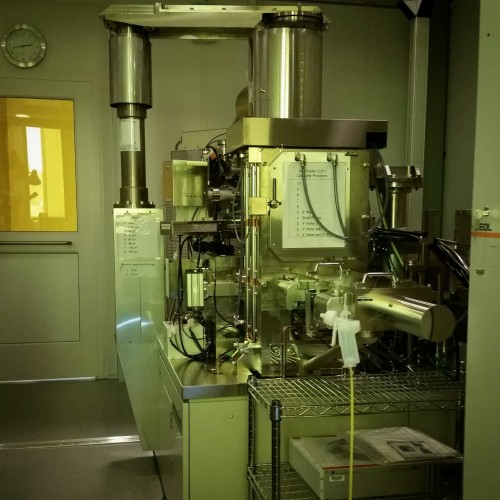
Electron beam lithography is a technique used to write nanometer-size features using a narrow beam of electrons to trace out the desired pattern on your sample. This is a form of maskless lithography - custom patterns can be written without the need for a mask. However, ebeam lithography has a low throughput and it is expensive, making it impractical for industrial purposes. This form of lithography is mainly used in research, mask writing, and prototyping, rather than for mass producing devices.
In the past, I have used this system to make nanowires that are less than 100 nm wide. This is 1/1000th the diameter of a human hair!
Post link


