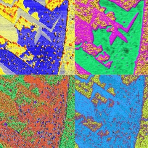
#atomic force microscopy
Extracting energy from a 60 nanometers thin layer
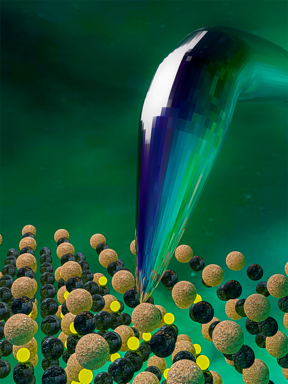
A team of researchers have demonstrated the viability of the direct piezoelectric effect in a thin film Bismuth Ferrite Material for the first time. The work, published in Nanoscale entitles “Direct and Converse Piezoelectric Responses at the Nanoscale from Epitaxial BiFeO3 Thin Films Grown by Polymer Assisted Deposition” which has gained the cover letter of such journal.
[…]
In this particular research, the BFO was scanned in a novel methodology named “Direct Piezoelectric Force Microscopy” DPFM, a new AFM mode invented in 2017
(https://www.nature.com/articles/s41467-017-01361-2 ). The material in this mode is stressed by the AFM tip with nanometric size. The tip applies a force in the range of hundreds of microNewton and measures the generated charge that is created by the material. For the case of BFO material, the piezoelectric characteristics were collected when the tip crosses antiparallel domain configurations, see the following video for a 3D representation of the tip crossing such configuration: https://youtu.be/ir3W2Vk8hCs
Post link
Novel monolayer ferroelectric hybrid structures
Scientists at the U.S. Naval Research Laboratory (NRL), Materials Science and Technology Division, have demonstrated that the intensity and spectral composition of the photoluminescence emitted from a single monolayer of tungsten disulphide (WS2) can be spatially controlled by the polarization domains in an adjacent film of the ferroelectric material lead zirconium titanate (PZT).
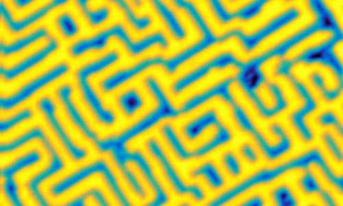
These domains are written in the PZT using a conductive atomic force microscope, and the photoluminescence (PL) is measured in air at room temperature. Because the polarization domain wall width in a ferroelectric can be as low as 1-10 nm, this approach enables spatial modulation of PL intensity and the corresponding carrier populations with potential for nanoscale resolution.
Single monolayer transition metal dichalcogenides (TMDs) such as WS2 exhibit striking optical properties due to their direct band gap. The dielectric screening is very low due to their two dimensional (2D) character, and thus their properties are strongly affected by their immediate environment, and can be modified and controlled by variations in local charge density due to adsorbates or electrostatic gating. This has generated keen interest in a wide variety of electronic and optical device applications.
Post link
New NIST method measures 3D polymer processing precisely
Recipes for three-dimensional (3D) printing, or additive manufacturing, of parts have required as much guesswork as science. Until now.
Resins and other materials that react under light to form polymers, or long chains of molecules, are attractive for 3D printing of parts ranging from architectural models to functioning human organs. But it’s been a mystery what happens to the materials’ mechanical and flow properties during the curing process at the scale of a single voxel. A voxel is a 3D unit of volume, the equivalent of a pixel in a photo.
Now, researchers at the National Institute of Standards and Technology (NIST) have demonstrated a novel light-based atomic force microscopy (AFM) technique – sample-coupled-resonance photorheology (SCRPR) – that measures how and where a material’s properties change in real time at the smallest scales during the curing process.
Post link
Imaging the chemical structure of individual molecules, atom by atom
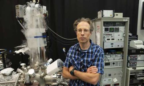
For physicist Percy Zahl, optimizing and preparing a noncontact atomic force microscope (nc-AFM) to directly visualize the chemical structure of a single molecule is a bit like playing a virtual reality video game. The process requires navigating and manipulating the tip of the instrument over the world of atoms and molecules, eventually picking some up at the right location and in the right way. If these challenges are completed successfully, you advance to the highest level, obtaining images that precisely show where individual atoms are located and how they are chemically bonded to other atoms. But take one wrong move, and it is game over. Time to start again.
“The nc-AFM has a very sensitive single-molecule tip that scans over a carefully prepared clean single-crystal surface at a constant height and "feels” the forces between the tip molecule and single atomsand bonds of molecules placed on this clean surface,“ explained Zahl, who is part of the Interface Science and Catalysis Group at the Center for Functional Nanomaterials (CFN), a U.S. Department of Energy (DOE) Office of Science User Facility at Brookhaven National Laboratory. "It can take an hour or days to get this sensor working properly. You can’t simply press a button; fine tuning is required. But all of this effort is definitely worthwhile once you see the images appearing like molecules in a chemistry textbook.”
Post link
Strange things happen when a crystal is split in two
The remarkable strength of ionic crystals is easily explained at the atomic scale: Positively and negatively charged atoms sit side by side in a repeating periodic arrangement. The strong electrostatic force in between keeps them together.
But what happens when the periodic pattern comes to an abrupt end? Researchers at the Vienna University of Technology have carefully broken potassium tantalate crystals in specific directions, and imaged the resulting surfaces using a state-of-the art atomic force microscope. Their data was combined with computations performed at the University of Vienna, and a series of remarkable phenomena were ultimately explained. The results were published in Science, and are potentially useful for technologies such as hydrogen production.
The black and white squares on a chess board alternate along the rows and columns, and at an angle from corner to corner, they appear as black and white rows. The black and white squares in two dimensions resemble a crystal in three dimensions: “If one splits a cubic crystal along a certain direction, one can end up with only positive or only negative charges at the surface. Such a situation would be highly unstable,” explains Prof. Ulrike Diebold of he Institute of Applied Physics of the Vienna University of Technology. A stacking of purely positive and negatively charged layers would result in a potential of millions of volts across the tiny sample—scientists call this the “polar catastrophe.” To avoid this situation, the atoms must reorganize. But how?
Post link
Study shows how calcium carbonate forms composites to make strong materials such as in shells and pearls
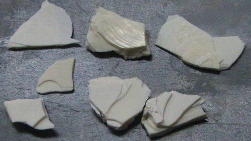
Seashells and lobster claws are hard to break, but chalk is soft enough to draw on sidewalks. Though all three are made of calcium carbonate crystals, the hard materials include clumps of soft biological matter that make them much stronger. A study today in Nature Communications reveals how soft clumps get into crystals and endow them with remarkable strength.
The results show that such clumps become incorporated via chemical interactions with atoms in the crystals, an unexpected mechanism based on previous understanding. By providing insight into the formation of natural minerals that are a composite of both soft and hard components, the work will help scientists develop new materials for a sustainable energy future, based on this principle.
“This work helps us to sort out how rather weak crystals can form composite materials with remarkable mechanical properties,” said materials scientist Jim De Yoreo of the Department of Energy’s Pacific Northwest National Laboratory. “It also provides us with ideas for trapping carbon dioxide in useful materials to deal with the excess greenhouse gases we’re putting in the atmosphere, or for incorporating light-responsive nanoparticles into highly ordered crystalline matrices for solar energy applications.”
Post link
Semi-Fluorinated Alcanes on HOPG.
Maps of Topography, Surface Potential, Dielectric response and dC/dV which were obtained using multiple lock-in scheme characterize local electrostatic properties at the nanometer scale.
Sample courtesy: Dr. M. Moeller (#DWI Aachen)
Image courtesy: Dr. Sergey Magonov, #ntmdt #next #afm #microscope #nanotechnology #polymers #science by ntmdt http://bit.ly/1J0iUkc
Post link
Discarded AFM tips.
Atomic Force Microscopy, or AFM, is a technique by which a small mechanical probe is scanned across a sample to create a height map. This technique has very high resolution, less than a nanometer, depending on what kind of tip is being used, and can be done in ambient conditions (no need for vacuum). AFM is useful for getting roughness data and measuring film thickness, and can be combined with other microscopy techniques to get a complete picture of your device.
AFM probes often get damaged or dirty, resulting in “tip graveyards” like the one shown here.
Post link

