#laboratory


Aspirin crystals.
Making new bone in the lab
Researchers at the University of Southampton are creating bone in the lab to help patients who suffer damage to their joints through injury or disease.
By combining bone stem cells with a 3D printed scaffold, Professor Richard Oreffo and team have been able to recreate hip implants custom designed for the patient.
There’s a place for synthetic implants, but by repairing your own body with your own tissue there is less chance of rejection.
In the video above you can see cells ‘proliferating’ or increasing in number. The team use and apply scaffolds in a range of materials, including titanium which are then seeded with the patient’s own bone stem cells and a bone graft. This 3D printed, custom designed implant can then be inserted into the patient.
There are tens of thousands of bone injuries in the UK each year. With an increasingly ageing population, this method for creating bone is an exciting concept. Professor Richard Oreffo hopes that given their data from 3 patients over the last 12 months, within 5-7 years the procedure could become mainstream, routine practice.
To read the full interview with Professor Oreffo visit: http://www.bbsrc.ac.uk/news/people-skills-training/2014/141106-f-gbbf-science-behind-exhibit-scaffold-and-cells/
A selection of evaporation sources in our cleanroom. Evaporation is a thin film deposition technique where the material is heated up to above its melting point in vacuum, typically using an electron beam. The molten material evaporates and is redeposited on your samples which are positioned near the source. Common materials that can be deposited using this technique include gold, copper, titanium, platinum, nickel, iron, silicon dioxide, and carbon.
Post link
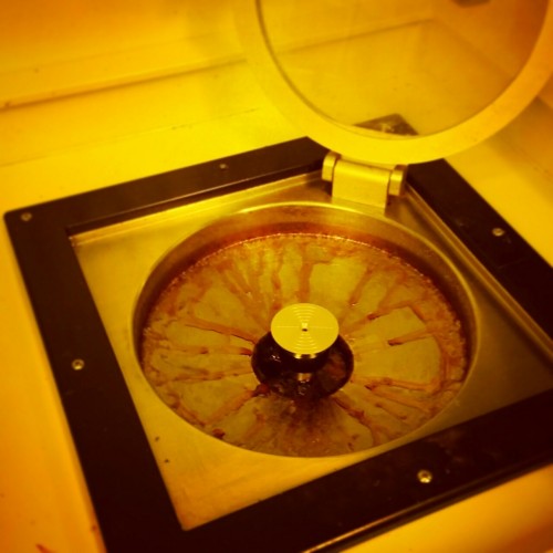
I spent part of the day today spinning photoresist. Photoresists are light sensitive chemicals used in photolithography. They are spun onto the sample at high speeds, using a tool like the one in the picture, to ensure an even coat. Yellow lighting is used in rooms dedicated to resist application and processing to prevent it from getting exposed. Once the resist is applied, a pattern can be transferred to your sample by exposing only certain areas to light.
Post link
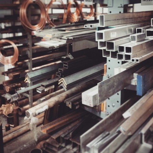
Metal stock in our department’s machine shop. Basic machining skills are often necessary to build an experiment, and so many experimental physicists are encouraged to take a course in machining. The final project is to make a nut and bolt from scratch.
Post link
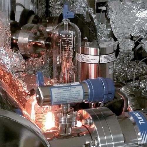
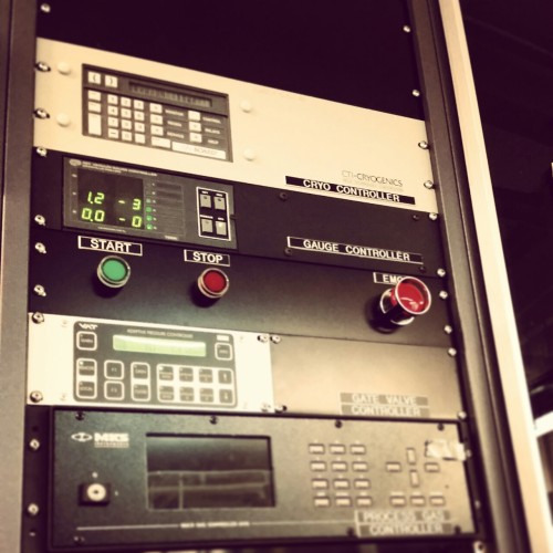
Ion gauges on one of our deposition systems.
Ionization gauges are commonly used to measure pressure in high vacuum. They look and operate very much like a light bulb. Electrons are emitted from a central heated filament (the glowing part) and accelerated toward a helical wire or “grid” around the filament. Some of these electrons collide with gas molecules and ionize them. The ions are then attracted to a collector filament, creating a current which can be measured. The magnitude of the ion current depends on the pressure and composition of the gas.
Post link
Aluminum target for our sputter system. If you look closely you can see individual crystal grains.
Sputtering is a technique used to deposit thin films of material. The material source is called a target because it is bombarded with high energy atoms which remove bits of material that are then redeposited on your sample or wafer. The ring is a result of the magnetic field confining the plasma to that region.
Post link
Discarded AFM tips.
Atomic Force Microscopy, or AFM, is a technique by which a small mechanical probe is scanned across a sample to create a height map. This technique has very high resolution, less than a nanometer, depending on what kind of tip is being used, and can be done in ambient conditions (no need for vacuum). AFM is useful for getting roughness data and measuring film thickness, and can be combined with other microscopy techniques to get a complete picture of your device.
AFM probes often get damaged or dirty, resulting in “tip graveyards” like the one shown here.
Post link
Sample stage controls for an ion mill, allowing for rotation about two different axes.
Ion milling is a type of dry etch process used to remove parts of a sample by bombarding it with ions, typically argon, in a vacuum chamber. It can be thought of as an atomic sand blaster. Ions (the “grains of sand”) physically expel, or sputter, chunks of material from the surface. The sample is rotated to ensure uniform coverage.
Post link
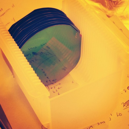
Patterned silicon wafers in the clean room.
Photolithography is a technique similar to photography used to make very small micron (~0.00004 inch) sized features. Wafers are coated in light sensitive chemicals called photoresist and then certain areas are exposed to light to create a pattern. The processing room is lit with yellow light to avoid exposing the resist. Photolithography is commonly used to make integrated circuits in electronics, but it is also used in basic research in fields such as physics, material science, engineering, and even biology.
Post link
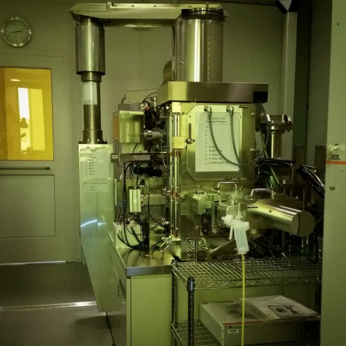
Electron beam lithography is a technique used to write nanometer-size features using a narrow beam of electrons to trace out the desired pattern on your sample. This is a form of maskless lithography - custom patterns can be written without the need for a mask. However, ebeam lithography has a low throughput and it is expensive, making it impractical for industrial purposes. This form of lithography is mainly used in research, mask writing, and prototyping, rather than for mass producing devices.
In the past, I have used this system to make nanowires that are less than 100 nm wide. This is 1/1000th the diameter of a human hair!
Post link
Togging room for our cleanroom.
Cleanrooms, often used in industrial and scientific research, are environments with a controlled number of particles of a certain size per unit area in the air. This is to prevent contamination of samples during fabrication - large particles can ruin electrical devices and decrease yield.
To decrease the number of particles in the air, researchers are required to wear full body “bunny suits” and certain particle-generating items, such as pencils and normal paper, are not allowed. The room is slightly pressurized and the flow of air is controlled to push particles toward the floor and out of the cleanroom.
Our cleanroom is Class 1000, meaning there is approximately 1/100th the number of particles in regular air.
Post link
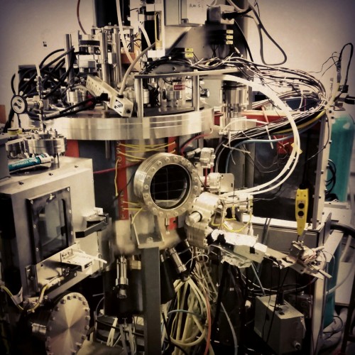
A sputter system in our lab.
Sputter deposition is a fabrication technique used to deposit thin films of a particular material onto a sample. The film can then be patterned using lithography into, for example, electrical contacts for your device. It is commonly used in the semiconductor industry to make integrated circuits.
First a gaseous plasma of ions, typically argon, is created in the sputter chamber. Ions in the plasma are then accelerated into a large piece of the material to be deposited, called the target, causing atoms to be ejected from the surface. Atoms that reach the sample or substrate are redeposited, forming a thin film over time.
Post link

Mermay Day 3 - “sweet”
sequel of yesterday, after she read Queenie the story of the little mermaid, the doc bought her a dress, so she can feel like a princess

Mermay Day 1 - “Angelic”
featuring “Shark Girl!”
Created in a secret goverment lab, Queenie was supposed to become a weapon. Half human, half shark and full of attitude.

