Researchers at the U.S. Department of Energy’s Lawrence Berkeley National Laboratory (Berkeley Lab) have developed a graphene device that’s thinner than a human hair but has a depth of special traits. It easily switches from a superconducting material that conducts electricity without losing any energy, to an insulator that resists the flow of electric current, and back again to a superconductor - all with a simple flip of a switch. Their findings were reported today in the journal Nature.
[…]
“Usually, when someone wants to study how electrons interact with each other in a superconducting quantum phase versus an insulating phase, they would need to look at different materials. With our system, you can study both the superconductivity phase and the insulating phase in one place,” said Guorui Chen, the study’s lead author and a postdoctoral researcher in the lab of Feng Wang, who led the study. Wang, a faculty scientist in Berkeley Lab’s Materials Sciences Division, is also a UC Berkeley physics professor.
On an otherwise normal day in the lab, Eva Andrei didn’t expect to make a major discovery. Andrei, a physics professor at Rutgers University, was using graphite – the material in pencils – to calibrate a scanning tunneling microscope. As part of the process, she turned on a very powerful magnetic field. When she looked up to see the material’s electronic spectrum, she was astonished. “We saw huge, beautiful peaks up there, just incredible. And they didn’t make any sense,” she recalled.
Remembering a lecture she’d recently attended, she realized the graphite had separated out into sheets just one atom thick. This material, known as graphene, has bizarre electronic properties. But even for graphene, the spectrum she saw was strange. In fact, no one had ever seen anything like it before. As Andrei described it, her colleague “went berserk in the corridor and just yelled ‘Graphene!’” Andrei had made a serendipitous discovery – a new electric phenomenon.
This was neither the first nor last time that electrons’ movement in graphene would surprise and elate scientists. One of the most impressive things about graphene is how fast electrons move through it. They travel through it more than 100 times faster than they do through the silicon used to make computer chips. In theory, this suggests that manufacturers could use graphene to make superfast transistors for faster, thinner, more powerful touch-screens, electronics, and solar cells.
Scientists at the U.S. Department of Energy’s Ames Laboratory were able to successfully manipulate the electronic structure of graphene, which may enable the fabrication of graphene transistors— faster and more reliable than existing silicon-based transistors.
The researchers were able to theoretically calculate the mechanism by which graphene’s electronic band structure could be modified with metal atoms. The work will guide experimentally the use of the effect in layers of graphene with rare-earth metal ions “sandwiched” (or intercalated) between graphene and its silicon carbide substrate. Because the metal atoms are magnetic the additions can also modify the use of graphene for spintronics.
“We are discovering new and more useful versions of graphene,” said Ames Laboratory senior scientist Michael C. Tringides. “We found that the placement of the rare earth metals below graphene, and precisely where they are located, in the layers between graphene and its substrate, is critical to manipulating the bands and tune the band gap.”
A group of scientists from Russia, the USA and China, led by Artyom Oganov from the Moscow Institute of Physics and Technology (MIPT), using computer generated simulation have predicted the existence of a new two-dimensional carbon material, a “patchwork” analogue of graphene called phagraphene. The results of their investigation were recently published in the journal Nano Letters.
“Unlike graphene, a hexagonal honeycomb structure with atoms of carbon at its junctions, phagraphene consists of penta-, hexa- and heptagonal carbon rings. Its name comes from a contraction of Penta-Hexa-heptA-graphene,” says Oganov, head of the MIPT Laboratory of Computer Design.
Two-dimensional materials, composed of a one-atom-thick layer, have attracted great attention from scientists in the last few decades. The first of these materials, graphene, was discovered in 2004 by two MIPT graduates, Andre Geim and Konstantin Novoselov. In 2010 Geim and Novoselov were awarded the Nobel Prize in physics for that achievement.
Due to its two-dimensional structure, graphene has absolutely unique properties. Most materials can transmit electric current when unbound electrons have an energy that corresponds to the conduction band of the material. When there is a gap between the range of possible electron energies, the valence band, and the range of conductivity (the so-called forbidden zone), the material acts as an insulator. When the valence band and conduction band overlap, it acts a conductor, and electrons can move under the influence of electric field.
Yesterday we saw how graphene can be used as a lubricant to make friction disappear. Today scientists reveal that the two-dimensional sheets of linked carbon atoms can be fashioned into hinges and springs to build microscale machines.
cornelluniversity researchers made the tiny devices using principles from kirigami, the ancient art of cutting and folding paper. Melina Blees and her colleagues decided to try the approach after early studies poking graphene sheets showed that the material behaves physically much like paper–it folds and crumples outside of the sheet’s plane but doesn’t stretch or compress within the plane. Learn more and see photos and video below.
(A large sheet of graphene can be crumpled like soft paper and returns to its original shape in a water and soap solution.)
Graphene Roll-Ups Make Friction Disappear, Could Revolutionize Machine Engineering
Chalk another amazing ability up for the supermaterial graphene. It seems the atom-thick sheets of linked carbon atoms can virtually eliminate friction.
The simulation above depicts the graphene-lubricant discovery–blue graphene sheets roll up to encase gold nanodiamonds as a surface of black diamond-like carbon slides over. Once the graphene wraps into so-called nanoscrolls around the nanodiamonds, the sheets make friction disappear.
“The nanoscrolls combat friction in very much the same way that ball bearings do by creating separation between surfaces,” said Argonne National Lab researcher Sanket Deshmukh. Learn more and see photos below.
Using powerful computer simulations, researchers from Brown University have identified a material with a higher melting point than any known substance.
The computations, described in the journal Physical Review B (Rapid Communications), showed that a material made with just the right amounts of hafnium, nitrogen, and carbon would have a melting point of more than 4,400 kelvins (7,460 degrees Fahrenheit). That’s about two-thirds the temperature at the surface of the sun, and 200 kelvins higher than the highest melting point ever recorded experimentally.
The experimental record-holder is a substance made from the elements hafnium, tantalum, and carbon (Hf-Ta-C). But these new calculations suggest that an optimal composition of hafnium, nitrogen, and carbon – HfN0.38C0.51 – is a promising candidate to set a new mark. The next step, which the researchers are undertaking now, is to synthesize material and corroborate the findings in the lab.
“The advantage of starting with the computational approach is we can try lots of different combinations very cheaply and find ones that might be worth experimenting with in the lab,” said Axel van de Walle, associate professor of engineering and co-author of the study with postdoctoral researcher Qijun Hong. “Otherwise we’d just be shooting in the dark. Now we know we have something that’s worth a try.”
Chemists are working to synthesize the next generation of super materials for high-performance electronics, solar cells, photodetectors and quantum computers. While they have made progress with compound materials, they have not yet succeeded in developing unaltered or “freestanding” materials for such devices, according to a review published in the journal Science and Technology of Advanced Materials.
Graphene is a carbon material derived from graphite, the same type of material found in pencils, but it is arranged in a one-atom-thin honeycomb lattice. Discovered in 2004, graphene’s two-dimensional arrangement gives it “extraordinary” properties, including extreme strength and “marvelously high” electron conductivity.
However, the tight lattice lacks a semiconducting bandgap, which is essential for electronic devices. Therefore, scientists have been hunting for alternative materials that have bandgaps, but still have a graphene-like structure.
Much focus has been placed on graphene quantum dots, which are small segments of graphene, about 10 to 100 nm carbon hexagons across and less than 30 atomic sheets thick. To make the dots behave more like 2-D graphene, research teams have added other molecules to change the structure and function of the material.
The Airbus A350 XWB and the Boeing 787-9 Dreamliner are currently perhaps the two most advanced passenger jets in the world.
They are both at the Paris Air Show, and they both carry GE technologies and materials. The GEnx engines that power the Dreamliner, for example, have fan blades and fan cases engineered from carbon fiber composites. The fixed trailing edge on the Airbus A350 XWB is made from a similar advanced material . In fact, more than a half of that jet’s body is made from composites.
“GE’s contribution to the structure of the A350 XWB plays a major role in the efficiency of the A350 wing fixed trailing edge,” says Mike Bausor, Airbus marketing director for the A350 XWB plane.“The [fixed trailing edge] is an integral part of the wing structure. Built predominantly from composite material, it is one of the most complex, highly loaded parts of the wing that requires utmost precision and mastery in the assembly process, as well as in the design and stress calculation.”
The fixed trailing edge makes the back part of the wing of the Airbus A350 XWB. Image credit: GE Reports/Adam Senatori.
Bausor says that composites are lighter than traditional aluminun alloys and also also extremely resistant. “But carbon fibre composite has other very valuable properties that bring major benefits to airlines,” he says. “This material does not corrode or fatigue. The maintenance tasks related to corrosion or fatigue on the airframe are therefore greatly reduced. The heavy maintenance interval can be extended to 12 years, versus 6 years for conventional airframes, significantly reducing maintenance cost and ensuring continued revenue generation for a much longer period.”
Both planes have been making afternoon flyovers at Paris Air Show this week. Photographer Adam Senatori captured some of the best moments.
Adam Senatori captured the A350 XWB (top) and the bird-like Boeing 787-9 Dreamliner (above) during flyovers at the Paris Air Show this week. Both planes feature GE materials and technologies. Image credits: GE Reports/Adam Senatori
The A350 XWB over Paris. Image credit: GE Reports/Adam Senatori
The Dreamliner in black & white. Image credit: GE Reports/Adam Senatori
Blink your eyes and it’s long gone. Carbonic acid exists for only a tiny fraction of a second when carbon dioxide gas dissolves in water before changing into a mix of protons and bicarbonate anions. Despite its short life, however, carbonic acid imparts a lasting impact on Earth’s atmosphere and …
A simple way to turn carbon nanotubes into valuable graphene nanoribbons may be to grind them, according to research led by Rice Univ. The trick, said Rice materials scientist Pulickel Ajayan, is to mix two types of chemically modified nanotubes. When they come into contact during grinding, they react and unzip, a process that until now has depended largely on reactions in harsh chemical solutions.
Nano-sized diamonds with certain defects are assetsfor people who study light.
Marko Loncar, an NSF-funded electrical engineer at Harvard School of Engineering and Applied Sciences, creates tiny structures out of diamonds and other elements to manipulate how light and matter interact on the nanoscale.
For instance, Loncar, who is part of the Nanoscale Interdisciplinary Research Team, uses diamond posts in a silver substrate as the scalable platform to enhance single photon emission by nitrogen vacancy centers in diamond.
Nitrogen vacancy centers are defects formed in diamonds that allow for the precise manipulation of absorbed photons and emitted light.
You may not want a flawed diamond on your finger, but it’s the defect that makes things like quantum computing possible.
Argonne scientists used Mira to identify and improve a new mechanism for eliminating friction, which fed into the development of a hybrid material that exhibited superlubricity at the macroscale for the first time. Argonne Leadership Computing Facility (ALCF) researchers helped enable the groundbreaking simulations by overcoming a performance bottleneck that doubled the speed of the team’s code.
While reviewing the simulation results of a promising new lubricant material, Argonne researcher Sanket Deshmukh stumbled upon a phenomenon that had never been observed before.
“I remember Sanket calling me and saying ‘you have got to come over here and see this. I want to show you something really cool,’” said Subramanian Sankaranarayanan, Argonne computational nanoscientist, who led the simulation work at the Argonne Leadership Computing Facility (ALCF), a DOE Office of Science User Facility.
They were amazed by what the computer simulations revealed. When the lubricant materials–graphene and diamond-like carbon (DLC)–slid against each other, the graphene began rolling up to form hollow cylindrical “scrolls” that helped to practically eliminate friction. These so-called nanoscrolls represented a completely new mechanism for superlubricity, a state in which friction essentially disappears.
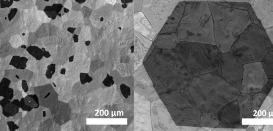
Researchers from the Nanomaterials by Design Group at University of Oxford, led by professor Nicole Grobert have produced millimetre-sized crystals of high-quality graphene in minutes, using a chemical vapour deposition technique (CVD).
The new method produces 2–3mm graphene crystals in 15 minutes, compared to current process which can take up to 19 hours.
Researchers took a thin film of silica deposited on a platinum foil which when heated, reacts to create a layer of platinum silicide. This layer melts at a lower temperature than platinum and silica to create a thin liquid layer that smooth’s out nanoscale ‘valleys’ in the platinum, so that carbon atoms in methane gas brushing the surface form large flakes of graphene.
Grobery, said, ‘Not only can we make millimetre-sized graphene flakes in minutes but this graphene is of a comparable quality to any other methods.’
The team believe the CVD technique could also have additional benefits claiming with a thicker liquid layer to insulate it the graphene might not have to be removed from the substrate before it can be used – an expensive and time consuming process.
Grobert added, ‘Of course a great deal more work is required before we get graphene technology, but we’re now on the cusp of seeing this material make the leap from the laboratory to a manufacturing setting, and we’re keen to work with industrial partners to make this happen.
The researchers hope to develop this technique further and produce flakes of graphene in large wafer-sized sheets.
To find out more on materials science, packaging and engineering news, visit our website IOM3 or follow us on Twitter @MaterialsWorld for regular news updates. You can also now get access to our content any time, anywhere via our app. For more information, visit app.materialsworld.org.
We found this video of the weird sound that aerogel makes if you drop it onto a hard surface*. It looks like it would be a squishy gel, but it’s actually hard like glass, and light as a feather. You can light a gas torch on one side and it won’t get hot enough to light a match sitting on the other side! Once you see this amazing substance for yourself, you’ll understand why some people call it “frozen smoke”.
*We don’t recommend dropping Aerogel. Its unique qualities make it fragile and prone to chip or break when roughly handled.
The difference between silicon aerogel an carbon aerogel is that carbon aerogel deforms plastically instead of shattering making it strong as steel and light as air ☼v☼
Like paper, graphene twists, folds into nanoscale machines
The art of kirigami involves cutting paper into intricate designs, like snowflakes. Cornell physicists are kirigami artists, too, but their paper is only an atom thick, and could become some of the smallest machines the world has ever known.
A research collaboration led by Paul McEuen, the John A. Newman Professor of Physical Science and director of the Kavli Institute at Cornell for Nanoscale Science (KIC), is taking kirigami down to the nanoscale. Their template is graphene, single atom-thick sheets of hexagonally bonded carbon, famous for being ultra thin, ultra strong and a perfect electron conductor. In the journal Nature July 29, they demonstrate the application of kirigami on 10-micron sheets of graphene (a human hair is about 70 microns thick), which they can cut, fold, twist and bend, just like paper.
Graphene and other thin materials are extremely sticky at that scale, so the researchers used an old trick to make it easier to manipulate: They suspended it in water and added surfactants to make it slippery, like soapy water. They also made gold tab “handles” so they could grab the ends of the graphene shapes. Co-author Arthur Barnard, also a Cornell physics graduate student, figured out how to manipulate the graphene this way.
“Cornell was a particularly great place to do this sort of work,” said the study’s first author, Melina Blees, a former physics graduate student and now a postdoctoral researcher at the University of Chicago. “I found an incredibly warm welcome in the art department, and the scientists were always genuinely excited about cross-disciplinary work in a way that’s still pretty rare,” she said.
A simple synthesis strategy could enable carbon nanomaterials to retain their unique properties in three-dimensions, say researchers. The team from Case Western Reserve University, Georgia Institute of Technology, University of North Texas, Air Force Research Laboratory in Dayton, Wenzhou Medical University, and Beijing Institute of Nanoenergy and Nanosystems has devised a novel one-step process to create seamless graphene—carbon nanotube (CNT) threedimensional nanostructures [Xue et al., Sci. Adv. (2015), 10.1126/sciadv.1400198].
One-dimensional carbon nanotubes and two-dimensional graphene boast impressive thermal, electrical, and mechanical properties in-plane but poor properties in three dimensions because of weak van der Waals interactions between layers. Now Liming Dai and colleagues have created hollow fibers consisting of radially aligned CNTs (RACNTs) attached to cylindrical graphene layers (Fig. 1) with a seamless junction between the two materials.
‘‘In our one-step process, the interface is made with carbon—to—carbon bonding so it looks as if it’s one single graphene sheet,’’ explains Dai. ‘‘That makes it an excellent thermal and electrical conductor in all planes.’’
High Definition images of Vertically Aligned NanoTube Arrays, or Vantablack - The Darkest known material since 2014.
info -
“vantablack is a substance made of carbon nanotubes and is the blackest substance known, absorbing a maximum of 99.965% of radiation in the visible spectrum. It comprises a forest of vertical tubes which are “grown”. When light strikes vantablack, instead of bouncing off, it becomes trapped and is continually deflected between the tubes before eventually becoming heat.Early development was carried out at the National Physical Laboratory, UK.” - wikipedia
Scientists at the U.S. Department of Energy’s Argonne National Laboratory have found a way to use tiny diamonds and graphene to give friction the slip, creating a new material combination that demonstrates the rare phenomenon of “superlubricity.” From left, researchers Ani Sumant, Ali Erdemir, Su…