#nitrides
Trapping gases better with boron nitride ‘nanopores’
What is common between a technology for storing energy in a solar cell and that for water purification? They both rely on the use of porous materials, or more specifically, 'nanoporous’ materials that can trap gas molecules within narrow spaces on their surface, called pores, which are only nanometers (one-billionth of a meter) in size. In the parlance of chemistry, the phenomenon is known as adsorption and has played an important role in the synthesis of porous materials of different compositions, pore sizes, and even pore geometries.
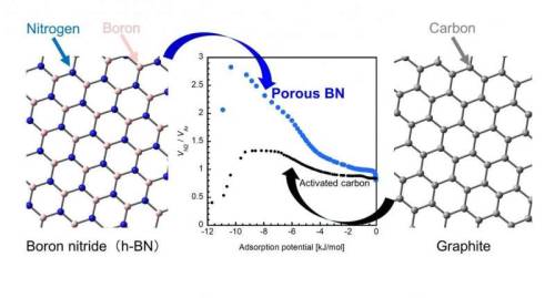
Traditionally, activated carbon (AC, or a porous form of carbon) has been a popular adsorbent for practical applications owing to its higher capacity of adsorption than that of other porous materials. Lately, however, porous boron nitride (p-BN) has emerged as a promising alternative because of its impressive performance, as highlighted by a recent study claiming that p-BN can adsorb a relatively large amount of carbon dioxide at room temperature.
Now, a group of scientists from Okayama University and Nagasaki University, Japan, has put this claim to the test in their latest study, where they examined the adsorbing characteristics of p-BN in detail. “A BN unit and two carbon atoms (i.e., CC) both have the same number of electrons and similar structures, but their interaction with gas molecules are different due to the atomically heterogeneous nature of BN. Despite this, there has been very little research on BN materials. In our study, we wanted to see if BN has specific adsorption properties that cannot be observed in carbon materials,” explains Dr. Takahiro Ohkubo from Okayama University, who led this study published in the journal RSC Advances.
Post link
Graphene-driving strain engineering to enable strain-free epitaxy of AlN film for deep ultraviolet light-emitting diode
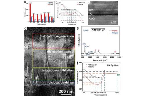
The direct band gap of AlN-based materials makes them suitable for fabricating DUV optoelectronic devices, which have a wide range of application prospects in the fields of curing, water and air disinfection, medicine and biochemistry. Therefore, achieving a high-quality epitaxy of AlN films is of particular importance to ensure the excellent performance of DUV photoelectric devices.
Currently, due to the lack of cost-effective homogenous substrates, the optimal choice to grow AlN films is usually to perform heteroepitaxial growth on sapphire. Unfortunately, the inherent mismatches between AlN and sapphire substrate inevitably introduce a variety of crystalline defects into the AlN epilayer. In particular, the large residual strain in the AlN film leads to the nonuniformity of the Al distribution in the upper AlGaN layer accompanied by wafer bending, which severely limits the device performance. Therefore, a feasible strategy is required to make a qualitative leap to realize high-quality growth of heteroepitaxial AlN films and to meet the application requirements of DUV optoelectronic devices.
Post link
Producing ammonia through electrochemical processes could reduce carbon dioxide emissions
Ammonia is commonly used in fertilizer because it has the highest nitrogen content of commercial fertilizers, making it essential for crop production. However, two carbon dioxide molecules are made for every molecule of ammonia produced, contributing to excess carbon dioxide in the atmosphere.
A team from the Artie McFerrin Department of Chemical Engineering at Texas A&M University consisting of Dr. Abdoulaye Djire, assistant professor, and graduate student Denis Johnson, has furthered a method to produce ammonia through electrochemical processes, helping to reduce carbon emissions. This research aims to replace the Haber-Bosch thermochemical process with an electrochemical process that is more sustainable and safer for the environment.
The researchers recently published their findings in Scientific Reports.
Since the early 1900s, the Haber-Bosch process has been used to produce ammonia. This process works by reacting atmospheric nitrogen with hydrogen gas. A downside of the Haber-Bosch process is that it requires high pressure and high temperature, leaving a large energy footprint. The method also requires hydrogen feedstock, which is derived from nonrenewable resources. It is not sustainable and has negative implications on the environment, expediting the need for new and environmentally friendly processes.
Post link
Aluminum on the way to titanium strength
NUST MISIS scientists have proposed a technology that can double the strength of composites obtained by 3-D printing from aluminum powder, and advance the characteristics of these products to the quality of titanium alloys: titanium’s strength is about six times higher than that of aluminum, but the density of titanium is 1.7 times higher.
The developed modifiers for 3-D printing can be used in products for the aerospace industry.
The developed modifying-precursors, based on nitrides and aluminum oxides and obtained through combustion, have become the basis of the new composite. The research results have been published in the highly rated scientific journal Sustainable Materials and Technologies.
Two decades ago, molding was considered the only cost-effective way to manufacture bulk products. Today, 3-D printers for metal are a worthy competitor to metallurgical methods. 3-D printers have a chance to replace traditional methods of metallurgical production in the future. Using additive technologies with 3-D printing creates a whole array of advantages, from creating more difficult forms and designs to the technology’s cheaper cost and theoretical edge.
Post link
Curbing the flammability of epoxy resin
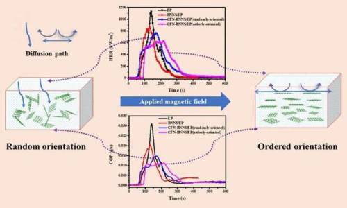
In a paper to be published in a forthcoming issue of Nano, a team of researchers from Henan University have investigated the flame retardant performance of epoxy resin using a boron nitride nanosheet decorated with cobalt ferrite nanoparticles.
Polymers are widely used in our daily lives due to good physical and chemical stability, corrosion resistance and other superior properties. However, most polymers, due to their organic nature, are inherently flammable which is a potential threat to the safety of human life and property. In order to avoid or reduce the flammability of polymers, it is a good strategy to add flame retardants to the polymers.
Among them, two-dimensional (2-D) layered inorganic nanomateirals (nanosheets), represented by graphene oxide,molybdenum disulfide, and boron nitride nanosheets (BNNS), exhibit excellent flame retardant performance due to their good physical barrier effects. However, the flame retardance is not enough in the use of such 2-D inorganic flame retardants alone, and in particular, the ability to suppress toxic gases and smoke is weak.
Post link
A graphene superconductor that plays more than one tune: Researchers at Berkeley Lab have developed a tiny toolkit for scientists to study exotic quantum physics
Researchers at the U.S. Department of Energy’s Lawrence Berkeley National Laboratory (Berkeley Lab) have developed a graphene device that’s thinner than a human hair but has a depth of special traits. It easily switches from a superconducting material that conducts electricity without losing any energy, to an insulator that resists the flow of electric current, and back again to a superconductor - all with a simple flip of a switch. Their findings were reported today in the journal Nature.
[…]
“Usually, when someone wants to study how electrons interact with each other in a superconducting quantum phase versus an insulating phase, they would need to look at different materials. With our system, you can study both the superconductivity phase and the insulating phase in one place,” said Guorui Chen, the study’s lead author and a postdoctoral researcher in the lab of Feng Wang, who led the study. Wang, a faculty scientist in Berkeley Lab’s Materials Sciences Division, is also a UC Berkeley physics professor.
Post link
Development of a transparent and flexible ultra-thin memory device
A two-dimensional (2D) nanomaterial-based flexible memory device is a critical element in the next-generation wearable market because it plays a crucial role in data storage, processing, and communication. An ultra-thin memory device materialized with a 2D nanomaterial of several nanometers (nm) can significantly increase the memory density, leading to the development of a flexible resistance-variable memory with the implementation of a 2D nanomaterial. However, memories using conventional 2D nanomaterials have limitations owing to the weak carrier trapping characteristics of the nanomaterials.
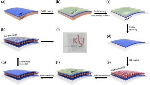
At the Institute of Advanced Composite Materials, Korea Institute of Science and Technology (KIST, President Yoon, Seok-Jin), a research team led by Dr. Dong-Ick Son announced the development of a transparent and flexible memory device based on a heterogeneous low-dimensional ultra-thin nanostructure. To this end, monolayered zero-dimensional (0D) quantum dots were formed and sandwiched between two insulating 2D hexagonal boron nitride (h-BN) ultra-thin nanomaterialstructures.
The research team materialized a device that could become a next-generation memory candidate by introducing 0D quantum dots with excellent quantum limiting properties into the active layer, controlling carriers in 2D nanomaterial. Based on this, 0D quantum dots were shaped in a vertically stacked composite structure that was sandwiched between 2D hexagonal h-BN nanomaterials to produce a transparent and flexible device. Therefore, the developed device maintains above 80% transparency and memory function even when bent.
Post link
Going cubic halves the efficiency droop in InGaAlN light-emitting diodes
Today, it is widely accepted that the large Auger coefficient is the main cause for the large (~50%) efficiency droop in traditional hexagonal-phase InGaAlN LEDs. Yet, this explanation is inadequate to account for the low efficiency droop in gallium arsenide- and gallium phosphide-based LEDs, as those have similar Auger coefficients.
InIEEE Transactions on Electron Devices, Can Bayram, Jean-Pierre Leburton and Yi-Chia Tsai at the University of Illinois at Urbana-Champaign show that the coexistence of strong internal polarization and large carrier effective mass accounts for ~51% of the efficiency droop under high current densities in hexagonal-phase green InGaAlN LEDs (h-LEDs) compared to cubic-phase InGaAlN green LEDs (c-LEDs).
Post link

