#semiconductors
By encoding information in photons via their spin, “photonic” computers could be orders of magnitude faster and efficient than their current-day counterparts. Likewise, encoding information in the spin of electrons, rather than just their quantity, could make “spintronic” computers with similar a…
Researchers have developed a new method for growing ‘hybrid’ crystals at the nanoscale, in which quantum dots – essentially nanoscale semiconductors – of different materials can be sequentially incorporated into a host nanowire with perfect junctions between the components. Images recorded in …
A well-known iron-based magnet is also a potential quantum information material
Scientists pursuing better performance in a well-known type of iron-based magnet also discovered wide-gap semiconducting behavior and a quantum state useful for quantum information processing—all in a single low-cost material that has been in existence for decades.
Scientists at the U.S. Department of Energy’s Critical Materials Institute, or CMI, study ways to make lower-cost, easier-to-obtain materials used as ingredients in technologies that are in demand now or are developing for the future. In this case, the researchers were investigating ways to create a stronger iron-based permanent magnet, something referred to as a “gap” magnet.
Permanent magnets fall into two broad categories. The strongest-performing permanent magnetscontainrare-earth metals like samarium, neodymium, and dysprosium—their properties make them the best and often only choice for applications like computer hard disk drives and motors in hybrid and electric vehicles. These magnets are typically expensive, and their rare-earth components can be difficult to obtain. The second, iron-based permanent magnets, are inexpensive and made of readily available materials, but their performance is often too poor for many advanced applications. In between the high performing rare-earth magnets and low-performing iron-based magnets is a “gap,” where there is a great need for permanent magnets that perform in the mid-range of desirable properties. Filling that gap reduces the need for rare-earth magnets, and in turn hard to source rare-earth materials.
Post link
World’s first white lasers demonstrated
While lasers were invented in 1960 and are commonly used in many applications, one characteristic of the technology has proven unattainable. No one has been able to create a laser that beams white light.
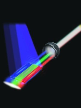
Researchers at Arizona State University have solved the puzzle. They have proven that semiconductor lasers are capable of emitting over the full visible color spectrum, which is necessary to produce a white laser.
The researchers have created a novel nanosheet – a thin layer of semiconductor that measures roughly one-fifth of the thickness of human hair in size with a thickness that is roughly one-thousandth of the thickness of human hair–with three parallel segments, each supporting laser action in one of three elementary colors. The device is capable of lasing in any visible color, completely tunable from red, green to blue, or any color in between. When the total field is collected, a white color emerges.
The researchers, engineers in ASU’s Ira A. Fulton Schools of Engineering, published their findings in the July 27 advance online publication of the journal Nature Nanotechnology. Cun-Zheng Ning, professor in the School of Electrical, Computer and Energy Engineering, authored the paper, “A monolithic white laser,” with his doctoral students Fan Fan, Sunay Turkdogan, Zhicheng Liu and David Shelhammer. Turkdogan and Liu completed their Ph.Ds. after this research.
Post link
An exotic material called gallium nitride (GaN) is poised to become the next semiconductor for power electronics, enabling much higher efficiency than silicon. In 2013, the Department of Energy (DOE) dedicated approximately half of a $140 million research institute for power electronics to GaN…
SCARY STORIES TO TELL IN THE LAB
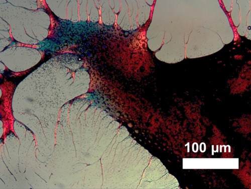
This image may look torn from the pages of a horror novel, but it actually depicts a possible new manufacturing method for electronic devices that work with living tissues. A team at Georgia Tech is studying the use of protein biofilms to direct the orderly formation of semiconducting polymer chains. Greater order in the chains could mean better and more predictable electronic properties for devices such as biocompatible sensors or electrodes. The researchers mixed poly(3-hexylthiophene) with a fungal protein called cerato-ulmin in the solvent 1,2,4-trichlorobenzene. As the proteins assembled into biofilms, the polymer collected in stable microstructures (dark areas above). These structures over time formed spindly branches, which slowly budded to release polymer-containing capsules. The team is now working on understanding and controlling the details of this process.
The resemblance to Stephen Gammell’s illustrations from the book series “Scary Stories to Tell in the Dark” is a happy accident.
Credit:Chem. Mater. 2015, DOI: 10.1021/acs.chemmater.5b04192
Post link
The material is called a silicene, a layer of silicon single atoms arranged in a honeycomb pattern that was first fabricated by researchers at UOW’s Institute for Superconducting and Electronic Materials (ISEM) and their partners in Europe and China. An ISEM team led by Professor Shi Xue Dou and …
Hexagonal boron nitride semiconductors enable cost-effective detection of neutron signals
One of the most critical issues the United States faces today is preventing terrorists from smuggling nuclear weapons into its ports. To this end, the U.S. Security and Accountability for Every Port Act mandates that all overseas cargo containers be scanned for possible nuclear materials or weapons.
Detecting neutron signals is an effective method to identify nuclear weapons and special nuclear materials. Helium-3 gas is used within detectors deployed in ports for this purpose.
The catch? While helium-3 gas works well for neutron detection, it’s extremely rare on Earth. Intense demand for helium-3 gas detectors has nearly depleted the supply, most of which was generated during the period of nuclear weapons production during the past 50 years. It isn’t easy to reproduce, and the scarcity of helium-3 gas has caused its cost to skyrocket recently – making it impossible to deploy enough neutron detectors to fulfill the requirement to scan all incoming overseas cargo containers.
Helium-4 is a more abundant form of helium gas, which is much less expensive, but can’t be used for neutron detection because it doesn’t interact with neutrons.
Printed electronics breakthrough could lead to flexible electronics revolution
A new form of electronics manufacturing which embeds silicon nanowires into flexible surfaces could lead to radical new forms of bendable electronics, scientists say.
In a new paper published today in the journal Microsystems and Nanoengineering, engineers from the University of Glasgow describe how they have for the first time been able to affordably ‘print’ high-mobility semiconductor nanowires onto flexible surfaces to develop high-performance ultra-thin electronic layers.
Those surfaces, which can be bent, flexed and twisted, could lay the foundations for a wide range of applications including video screens, improved health monitoring devices, implantable devices and synthetic skin for prosthetics.
The paper is the latest development from the University of Glasgow’s Bendable Electronics and Sensing Technologies (BEST) research group, led by Professor Ravinder Dahiya.
Post link
Something New Grows on Trees: Biodegradable Chips for Electronics
It was just a couple of weeks ago when we featured nanocellulose, a natural supermaterial derived from plants that is getting ready for the spotlight. Researchers are looking at it for durable, transparent composites because of its strength. Others are investigating its use in applications from biocompatible implants and flexible displays and solar panels to better bioplastics, cosmetics and concrete.
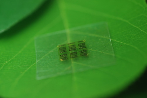
Now we hear from the University of Wisconsin-Madison and the U.S. Department of Agriculture Forest Products Laboratory that scientists have demonstrated a new product for the nanoscopic fibers of cellulose, a carbohydrate that gives structure to plant cell walls. Turning the material into a film, they’ve been able to produce high-performance computer chips made almost entirely of wood.
By replacing the semiconducting foundation of modern chips with biodegradable nanocellulose, electronics could become significantly less of an environmental burden when they are discarded.
Post link
New electronics? Black Phosphorus Reveals Its Secrets
A team of researchers from Université de Montréal, Polytechnique Montréal and the Centre national de la recherche scientifique (CNRS) in France is the first to succeed in preventing two-dimensional layers of black phosphorus from oxidating. In so doing, they have opened the doors to exploiting their striking properties in a number of electronic and optoelectronic devices. The study’s results were published in the prestigious journal Nature Materials.
Black phosphorus: future key player in new technologies Black phosphorus, a stable allotrope of phosphorus that presents a lamellar structure similar to that of graphite, has recently begun to capture the attention of physicists and materials researchers. It is possible to obtain single atomic layers from it, which researchers call 2D phosphane. A cousin of the widely publicized graphene, 2D phosphane brings together two very sought-after properties for device design.
First, 2D phosphane is a semiconductor material that provides the necessary characteristics for making transistors and processors. With its high-mobility, it is estimated that 2D phosphane could form the basis for electronics that is both high-performance and low-cost.
Furthermore, this new material features a second, even more distinctive, characteristic: its interaction with light depends on the number of atomic layers used. One monolayer will emit red light, whereas a thicker sample will emit into the infrared. This variation makes it possible to manufacture a wide range of optoelectronic devices, such as lasers or detectors, in a strategic fraction of the electromagnetic spectrum.
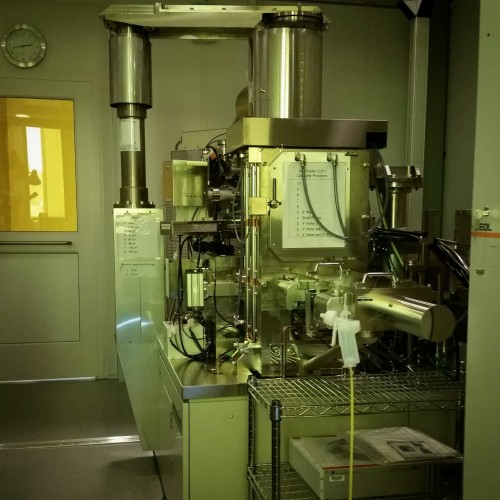
Electron beam lithography is a technique used to write nanometer-size features using a narrow beam of electrons to trace out the desired pattern on your sample. This is a form of maskless lithography - custom patterns can be written without the need for a mask. However, ebeam lithography has a low throughput and it is expensive, making it impractical for industrial purposes. This form of lithography is mainly used in research, mask writing, and prototyping, rather than for mass producing devices.
In the past, I have used this system to make nanowires that are less than 100 nm wide. This is 1/1000th the diameter of a human hair!
Post link
Togging room for our cleanroom.
Cleanrooms, often used in industrial and scientific research, are environments with a controlled number of particles of a certain size per unit area in the air. This is to prevent contamination of samples during fabrication - large particles can ruin electrical devices and decrease yield.
To decrease the number of particles in the air, researchers are required to wear full body “bunny suits” and certain particle-generating items, such as pencils and normal paper, are not allowed. The room is slightly pressurized and the flow of air is controlled to push particles toward the floor and out of the cleanroom.
Our cleanroom is Class 1000, meaning there is approximately 1/100th the number of particles in regular air.
Post link
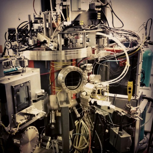
A sputter system in our lab.
Sputter deposition is a fabrication technique used to deposit thin films of a particular material onto a sample. The film can then be patterned using lithography into, for example, electrical contacts for your device. It is commonly used in the semiconductor industry to make integrated circuits.
First a gaseous plasma of ions, typically argon, is created in the sputter chamber. Ions in the plasma are then accelerated into a large piece of the material to be deposited, called the target, causing atoms to be ejected from the surface. Atoms that reach the sample or substrate are redeposited, forming a thin film over time.
Post link


